1 Introduction
Light emitting diodes (LEDs) are recognized as the next generation of lighting sources, but their general illumination still needs to further reduce costs and improve luminous efficiency. The successful development of GaN-based LEDs on silicon substrates has rewritten the history of GaN-based LEDs based on sapphire and silicon carbide, which has greatly reduced the manufacturing cost of LEDs. In order to improve the luminous efficiency of the LED, in addition to improving the internal quantum efficiency and the extraction efficiency, the operating voltage of the LED is also lowered under the same current, that is, the ohmic contact performance between the metal electrode and the LED film is improved. Due to the problem that the Mg acceptor is difficult to activate in p-GaN, the low hole concentration becomes a bottleneck restricting the p-type ohmic contact. Most of the literature uses a method of annealing at about 700 °C in an N2 atmosphere or annealing at about 500 °C in an atmosphere of oxygen to activate the Mg acceptor. In 2001, Waki ​​et al. first proposed the method of “successing Ni on the epitaxial layer to activate Mg acceptor in p-GaNâ€, and obtained a hole concentration of up to 7 × 1017 cm -3 . The process of "sacrificial Ni" is as follows: 1) evaporating the Ni cap layer on the surface of p-GaN on the sapphire substrate; 2) annealing it in the N2 atmosphere at a temperature ranging from 200 °C to 800 °C for 10 min; 3) removing Ni coating layer on the surface of the film; 4) Preparation of Ni/p-GaN ohmic contact layer; 5) Second annealing in a N2 atmosphere at a temperature of 550 °C. This method of activating Mg acceptors by sacrificial metal annealing has the characteristics of low activation temperature and easy integration with other processes. Later, many research groups used Ni, Co, Pt, Ti, Ti / Au and other H materials as sacrificial metals to selectively activate p-GaN on sapphire substrates, which improved the luminous efficiency and reliability of the device. In this paper, the effect of Ni cladding thickness and annealing temperature on the p-type ohmic contact of GaN-based LED films on silicon substrates was systematically investigated. A high-performance p-type ohmic contact layer was obtained without secondary annealing.
2. Experiment
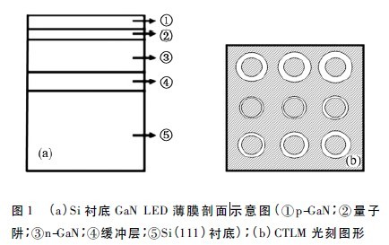
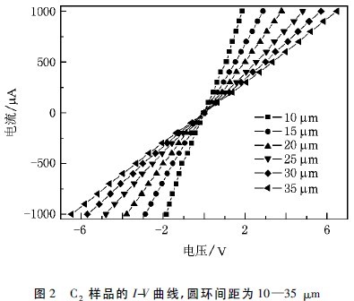
The sample used in this paper is a GaN-based LED epitaxial wafer on silicon substrate developed by the laboratory. The epitaxial structure is shown in Figure 1 (a). In order to avoid the influence of different epitaxial structures on the experimental results, this paper selects six epitaxial wafers of the same heat, labeled A, B, C, D, E, F. The sample is cleaned, blow dried, and subsequently evaporated by electron beam. 5,5. 5 nm, 5.0 nm, 15 nm, 45 nm thick Ni, A sample surface does not evaporate. Each sample was then divided into five equal parts and numbered: A1, A2, .... Then all the samples were divided into five groups according to the label, and annealed at 400 °C, 450 °C, 550 °C, 650 °C, 750 °C, respectively. The annealing atmosphere is N2: O2 = 4: 1, and the annealing time is 20 min. The details of annealing and labeling are shown in Table 1. After annealing, all samples were boiled in aqua regia for 20 min to remove nickel and nickel oxide from the surface of the sample. Subsequently, electron beam evaporation was used to evaporate 80 nm of Pt on all sample surfaces. After circular ray lithography (CTLM) lithography, the IV curve of each sample was tested and the sheet resistance (Rsh) and specific contact resistivity (Ïc) were calculated. . The CTLM lithography pattern is shown in Figure 1 (b). The ring spacing is 35 μm, 30 μm, 25 μm, 20 μm, 15 μm, 10 μm, 5 μm, 2. 5 μm. For the calculation of the IV curve of the C2 sample Rsh and Ïc, the ring spacing is 10-35 μm. Considering the lithography error, the rings with intervals of 5 μm and 2.5 μm are not tested.
3. Results and discussion
Table 1 lists the Ni overlay thickness (D), annealing temperature (T), sheet resistance (Rsh) of the p-type material, and Pt / p-GaN specific contact resistivity (Ïc) for each sample. It can be seen from the table that the Ïc (= 6. 1 × 10 - 5 Ω·cm2 ) of the C2 sample is the smallest, while the Rsh (= 9. 0 × 104 Ω) is the smallest, and Ïc is close to the best result reported in the literature of the same type. After annealing, the p-type layer Rsh is on the order of 105, which is consistent with the results reported in the literature. The Rsh and Ïc data of samples A1, E1, and F1 were not measured in this experiment. The reason was attributed to the fact that the Mg acceptors were not activated enough at the lower annealing temperature, Rsh was too large, and the current was difficult to expand. The p-GaN thickness of all samples in this experiment is only about 100 nm. The larger current in the I-V test is more difficult to extend along the lateral direction of the p-type material, which is the main reason for the large magnitude of the sheet resistance of the p-type material after annealing. .
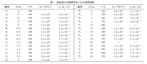
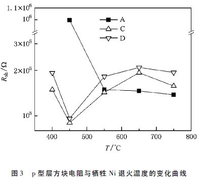
Figure 3 is a graph showing the annealing temperature of Rsh and sacrificial Ni of A, C, and D samples. The smaller the Rsh, the higher the hole concentration of the p-type layer and the greater the activation of the Mg acceptor. Rsh of sample A without sacrificial Ni annealing decreases with increasing annealing temperature, indicating that the activation degree of Mg acceptor increases with temperature; when the temperature is higher than 550 °C, Rsh continues to decrease, but the trend Significantly slower, indicating that the activation temperature of the Mg acceptor is about 550 °C when annealed directly in an aerobic atmosphere. The Rsh of the C and D samples with sacrificial Ni annealing decreases first and then increases with the increase of annealing temperature, and the inflection point appears at about 450 °C, indicating that the activation temperature of Mg acceptor is about 450 °C during sacrificial Ni annealing; C2, The Rsh values ​​of D2 samples are smaller than the Rsh values ​​of A4 samples, indicating that sacrificial Ni annealing can significantly reduce the activation temperature of Mg acceptors and increase the activation degree of Mg acceptors. The Rsh of C and D samples decreases first and then increases with the increase of annealing temperature. The explanation is as follows: At lower temperature, the activation of Mg acceptor is not enough, the hole concentration is low, and Rsh is large; The increase of Ni can significantly increase the desorption of H in the p-GaN film, and the Mg acceptor activation is significantly improved, and Rsh is significantly decreased. When the annealing temperature continues to increase, Ni promotes the formation of N vacancies. When the annealing temperature is between 460 and 700 °C, the concentration of Ni promoted the formation of N vacancies is about 3 × 1019 cm -3 , which largely compensates for the concentration of holes in the p-type material, which makes Rsh increase again.