
Since the frequency of the modulated signal is much lower than that of the carrier signal, its value changes very little over several cycles of the carrier. As a result, it can be considered nearly constant during this period. At this point, the amplitude-modulated signal (us) and the carrier signal (uc or Uc) are at the same frequency. When the modulation signal is positive, us and uc are in phase; when negative, they are out of phase. To determine the phase of the modulated signal, a phase-sensitive detection circuit is essential. This circuit not only receives the amplitude-modulated signal but also requires a reference signal of the same frequency as the carrier. The output voltage of the phase-sensitive detector indicates the phase relationship between the input signal and the reference: a positive voltage means the signals are in phase, while a negative voltage suggests they are out of phase.
Three different phase-sensitive detection circuits were simulated using Multisim, and the results are presented below.
1. Simulation Experiments 1.1, Scheme OneThe first simulation circuit is an additive phase-sensitive detection setup, shown in Figure 1. It uses ideal components, with the amplitude-modulated signal (us) input through transformer T1 and the reference signal (uc) through transformer T2. The reference signal has a much higher amplitude than the modulated signal. The output is a low-frequency signal, which is filtered by a capacitor to extract the demodulated signal. The simulation results are illustrated in Figure 2. In Figure 2(a), the signals are in phase, while in Figure 2(b), they are out of phase.
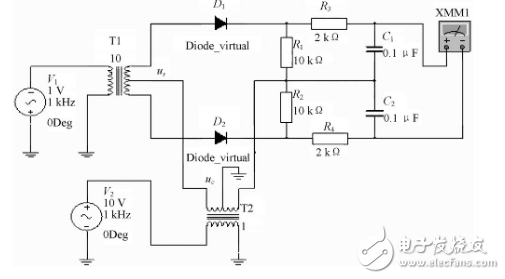
Figure 1: Additive half-wave phase-sensitive detection simulation circuit
1.2, Scheme TwoThe second simulation involves a switching full-wave phase-sensitive detection circuit, as shown in Figure 3. This design uses real components, where the reference signal (uc) is a square wave. During the high half-cycle of uc, the analog switch is on, resulting in a gain of -1. During the low half-cycle, the switch is off, and the gain becomes +1. The waveform results are displayed in Figure 4. In Figure 4(a), us and uc are in phase, while in Figure 4(b), they are out of phase.

Figure 2: Simulation operation result of phase-added phase sensitive detection circuit
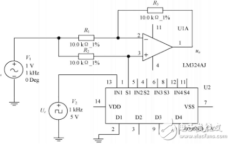
Figure 3: Switching full-wave phase-sensitive detection simulation circuit
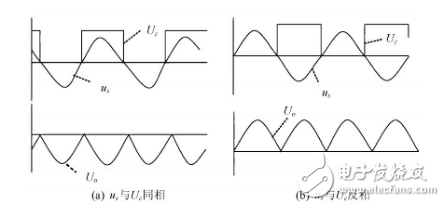
Figure 4: Switching full-wave phase-sensitive detection circuit simulation running waveform
1.3, Scheme ThreeThe third circuit, shown in Figure 5, is capable of identifying whether one signal leads or lags another. The output voltage reflects the phase difference between the two signals. A1 and A2 are zero-crossing comparators that convert the input signals into rectangular waves with the same phase difference. These signals are then processed through an XOR gate and a low-pass filter to generate a DC voltage proportional to the phase difference. This voltage is further amplified by A3. A D flip-flop and a transistor form a lead-lag identification circuit. When uA leads uB, the flip-flop outputs a high level, turning on the transistor and producing a negative output. Conversely, when uA lags uB, the flip-flop outputs a low level, turning off the transistor and producing a positive output. A phase-shifting network consisting of two equal-amplitude power sources (u1, u2) and a resistor-capacitor (R1, C1) is used to adjust the phase difference between uA and uB. The phase angle φ is given by φ = 2θ = 2arctg(ωR1C1). Figures 7 and 8 show the simulation results for R1 set to 1 kΩ and the corresponding waveforms at various points in the circuit.
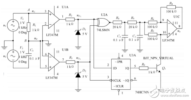
Figure 5: Phase sensitive detection simulation circuit
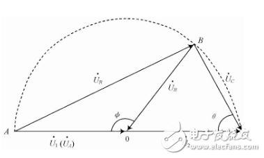
Figure 6: Phasor diagram

Figure 7: Output voltage of the circuit when R1 is 1kΩ
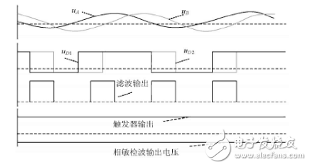
Figure 8: Waveform of each point in the circuit
2. ConclusionElectronic Design Automation (EDA) technology significantly reduces the design cycle, improves efficiency, lowers risks, and enhances the quality of electronic circuits. It also provides a powerful platform for experimental work. While simulations cannot fully replace physical experiments, they offer a convenient, fast, intuitive, and safe way to test and develop new projects. Using tools like Multisim, students and engineers can create more effective and innovative experimental setups.
Timing Belt,Lift Door Machine Belt,Elevator Door Machine Belt,Elevator Timing Belt
Shanghai Janetec Electric Co., Ltd. , https://www.janetecelectric.com