
To suppress EMI, the EMI design of digital circuits should be based on the following principles:
According to the relevant EMC/EMI technical specifications, the indicators are decomposed into single-board circuits and hierarchically controlled.
Controlling from the three aspects of EMI, namely interference source, energy coupling path and sensitive system, the circuit has a flat frequency response to ensure normal and stable operation of the circuit.
Start with the front-end design of the device, focus on EMC/EMI design, and reduce design costs.
2 EMI control technology for digital circuit PCB
When dealing with various forms of EMI, specific problems must be analyzed. In the PCB design of digital circuits, EMI control can be performed from the following aspects.
2.1 Device Selection
When designing an EMI, first consider the rate at which the device is selected. For any circuit, if a device with a rise time of 5ns is replaced with a device with a rise time of 2.5ns, the EMI will increase by about 4 times. The radiant intensity of EMI is proportional to the square of the frequency. The highest EMI frequency (fknee), also known as the EMI emission bandwidth, is a function of signal rise time rather than signal frequency:   
Fknee =0.35/Tr (where Tr is the signal rise time of the device)  
This type of radiated EMI has a frequency range of 30MHz to several GHz. In this band, the wavelength is very short, and even a very short wiring on the board can become a transmitting antenna. When EMI is high, the circuit tends to lose its normal function. Therefore, in the device selection, under the premise of ensuring the performance requirements of the circuit, low-speed chips should be used as much as possible, and appropriate driving/receiving circuits should be used. In addition, since the lead pins of the device have parasitic inductance and parasitic capacitance, the influence of the device package on the signal can not be ignored in the high-speed design, because it is also an important factor in generating EMI radiation. In general, the parasitic parameters of the SMD device are smaller than those of the interposer, and the parasitic parameters of the BGA package are smaller than the QFP package.   
2.2 Connector selection and signal terminal definition   
The connector is a key link in high-speed signal transmission and a weak link that is prone to EMI. The ground pin can be arranged on the connector's terminal design to reduce the signal-to-ground spacing, reduce the effective signal loop area of ​​the radiation generated in the connector, and provide a low-impedance return path. When necessary, consider isolating some key signals with ground pins.   
2.3 Laminated design   
Under the premise of cost, increase the number of ground planes, and reduce the EMI radiation by placing the signal layer close to the ground plane. For high-speed PCBs, the power and ground planes are immediately coupled to reduce power supply impedance and reduce EMI.  
2.4 Layout  
According to the signal current flow direction, a reasonable layout can be used to reduce interference between signals. Reasonable layout is the key to controlling EMI. The basic principles of layout are:
Analog signals are susceptible to interference from digital signals, and analog circuits should be separated from digital circuits;
The clock line is the main source of interference and radiation, away from sensitive circuits and keeping the clock traces to a minimum;
High-current, high-power circuits should be avoided in the center of the board as much as possible, and the effects of heat dissipation and radiation should be considered.
The connector should be arranged on one side of the board as far as possible and away from the high frequency circuit;
The input/output circuit is close to the corresponding connector, and the decoupling capacitor is close to the corresponding power pin;
Fully consider the feasibility of layout for power splitting, multi-supply devices should be placed across the boundaries of the power split region to effectively reduce the impact of planar splitting on EMI;
The reflow plane (path) is not split.
2.5 wiring
Impedance Control: High-speed signal lines present the characteristics of the transmission line and require impedance control to avoid signal reflection, overshoot and ringing, and reduce EMI emissions.
The signals are classified according to the EMI radiation intensity and sensitivity of different signals (analog signals, clock signals, I/O signals, buses, power supplies, etc.), so that the interference source and the sensitive system are separated as much as possible, and the coupling is reduced.
Strictly control the trace length of the clock signal (especially the high-speed clock signal), the number of vias, the cross-segment, the termination, the wiring layer, the return path, and so on.
The signal loop, the loop from which the signal flows out to the inflow of the signal, is the key to EMI control in the PCB design and must be controlled during routing. To understand the flow of each critical signal, route the critical signal close to the return path to ensure that its loop area is minimal.
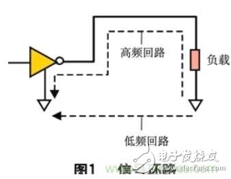
For low-frequency signals, the current must flow through the path with the least resistance; for high-frequency signals, the high-frequency current must flow through the path with the smallest inductance, not the path with the least resistance (see Figure 1). For differential mode radiation, the EMI radiation intensity (E) is proportional to the current, the area of ​​the current loop, and the square of the frequency. (where I is the current, A is the loop area, f is the frequency, r is the distance from the center of the loop, and k is a constant.)   
Therefore, when the minimum inductance return path is just below the signal conductor, the current loop area can be reduced, thereby reducing EMI radiant energy.
Critical signals must not cross the segmentation area.
High-speed differential signal traces are as tightly coupled as possible.
Make sure the strip line, microstrip line, and its reference plane meet the requirements.
The lead-out of the decoupling capacitor should be short and wide.
All signal traces should be as far as possible from the edge of the board.
For multi-drop networks, choose the appropriate topology to reduce signal reflections and reduce EMI emissions.  
2.6 Power plane segmentation processing
Power layer segmentation  
When there is one or more sub-power supplies on a main power plane, ensure the continuity of each power supply area and sufficient copper foil width. The dividing line does not have to be too wide, generally 20 to 50 mils line width to reduce the gap radiation.
Ground layer segmentation
The ground plane should maintain integrity and avoid segmentation. If it is necessary to divide, distinguish between digital ground, analog ground and noisy ground, and connect to the external ground through a common grounding point at the exit.  
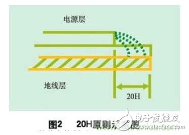
In order to reduce the edge radiation of the power supply, the power/ground plane should follow the 20H design principle, that is, the ground plane size is 20H larger than the power plane size (see Figure 2), so that the fringe field radiation intensity can be reduced by 70%.
3 Other control methods for EMI  
3.1 Power System Design
Design a low-impedance power system to ensure that the impedance of the power distribution system below the fknee frequency is below the target impedance.
Use a filter to control conducted interference.
Power supply decoupling. In EMI design, providing reasonable decoupling capacitors can make the chip work reliably, reduce high frequency noise in the power supply, and reduce EMI. Due to the influence of wire inductance and other parasitic parameters, the power supply and its power supply wire have a slow response speed, which may cause insufficient instantaneous current required by the driver in the high speed circuit. Properly design the bypass or decoupling capacitors and the distributed capacitance of the power plane to quickly supply current to the device using the energy storage of the capacitor before the power supply responds. Proper capacitive decoupling provides a low impedance power path, which is key to reducing common mode EMI.
3.2 Grounding
Grounding design is the key to reducing overall EMI.
Make sure to use single point grounding, multi-point grounding or hybrid grounding.
Digital ground, analog ground, and noise ground are separated and a suitable common ground point is determined.
If the double-panel design has no ground layer, it is important to design the ground grid properly. The width of the ground line should be guaranteed. Large-area paving can also be used, but it should be noted that the coherence of large areas on the same floor is better.
For multi-layer board design, ensure that there is a ground plane to reduce the common ground impedance.  
3.3 series damping resistor  
Under the premise of the circuit timing requirements, the basic technology for suppressing the interference source is to connect a small resistance value to the key signal output terminal, usually using a resistor of 22 to 33 Ω. These series-connected small resistors can slow down/fall time and make the overshoot and undershoot signals smoother, thus reducing the high-frequency harmonic amplitude of the output waveform and effectively suppressing EMI.
3.4 Shielding
EMI shielding materials or screens can be used for critical components.
Shielding of critical signals can be designed as striplines or isolated on the sides of critical signals by ground.  
3.5 Spread Spectrum  
Spread spectrum (spread spectrum) is a new and effective way to reduce EMI. Spread spectrum modulates a signal to spread the signal energy over a wide frequency range. In fact, this method is a controlled modulation of the clock signal, which does not significantly increase the jitter of the clock signal. Practical applications have proven that spread spectrum technology is effective and can reduce radiation by 7 to 20 dB.
3.6 EMI Analysis and Testing
Simulation analysis
After the PCB layout is completed, the EM I simulation software and expert system can be used for simulation analysis to simulate the EMC/EMI environment to evaluate whether the product meets the relevant EMC standards.
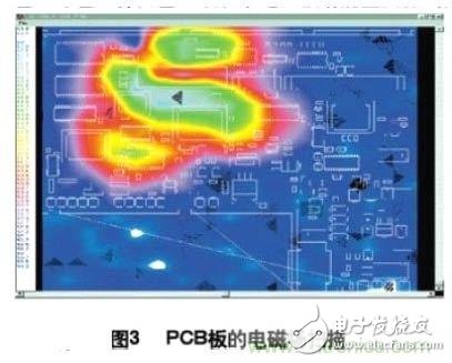
Scan test
The electromagnetic radiation scanner is used to scan the machine board after being assembled and powered up to obtain the electromagnetic field distribution map in the PCB (as shown in Fig. 3, the red, green and blue-white areas indicate the electromagnetic radiation energy from low to high), according to the test. The result is improved PCB design.
4 Summary
As new high-speed chips continue to be developed and applied, the signal frequency is getting higher and higher, and the PCB boards carrying them may become smaller and smaller. PCB design will face even more severe EMI challenges. Only by continuously exploring and innovating can the EMC/EMI design of PCB boards be successful.
HAODA ELECTRONIC CO.,LIMITED , https://www.pcbhdi.com