
introduction
Most of the contemporary LCD displays use a cold cathode ray fluorescent (CCFL) backlight or an LED static backlight. Due to the difficulty in controlling the brightness of the CCFL and the slow response, energy waste and dynamic blurring are caused. Although the LED static backlight effect is good, its energy consumption is also serious. In addition, the constant brightness backlight reduces the contrast of the image, and the display effect is not satisfactory. By analyzing the RGB pixels of the image and appropriately using the LED backlight with a lower brightness in some areas, it can not only save energy, but also enlarge the contrast of the image display and eliminate the dynamic blur phenomenon.
1 Design plan and its principle
The dynamic backlight is a whole on the surface. In fact, the interior has been divided into multiple areas when the schematic is made, and their respective brightness is controlled. It can be seen that the higher the density of the backlight, the more the divided areas and the smaller the area, the better the overall effect will be displayed. However, considering the cost, economic value, production process, energy saving and other aspects, it can be seen that the number of lamps cannot be infinitely large, and the divided areas are not infinitely dense, but one of the most suitable design specifications can always be found.
The RGB color model is a color standard in the industry that assigns an intensity value in the range of 0 to 255 for the RGB component of each pixel in the image through the RGB model. RGB images use only three colors, mixed in different proportions, theoretically presenting 16,777,216 colors on the screen. In this system, only the RGB components can not directly get the brightness control parameter Ki we need, and the gray value of each pixel of the image needs to be calculated by FPGA, and then calculated.
The basic idea of ​​grading the image is to average the values ​​of the RGB three color components of each pixel. However, due to the sensitivity of the human eye, this method is not effective. It should be that each component needs to have a certain value. The weight is calculated as shown below.
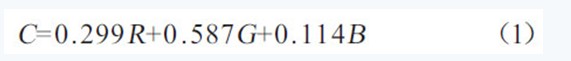
(1) For the gradation calculation formula, the gradation value of the pixel can be directly calculated from each component of RGB, and of course, the whole can be enlarged or reduced, that is, multiplied by a common coefficient.
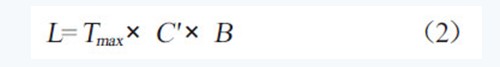
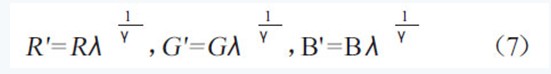
(2) In order to obtain the brightness formula from the pixel gray scale, where Tmax is the maximum transmittance, it is a fixed value in the same system, and can be ignored, γ is the RGB pixel correction factor, and B is the backlight brightness value.
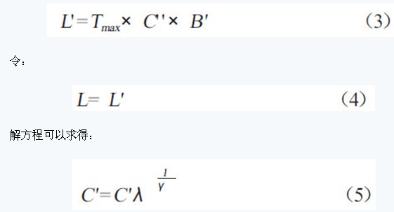
When the brightness of the backlight becomes 1/λ or B' of the original, in order to make the brightness of the gray-scale C' pixel not greatly change by the human eye, the values ​​obtained twice should be the same, namely:
make:
Solving the equation can be obtained:
In general, the adjustment of gray scale is controlled by 8-bit data, that is, the gray value can be divided into 256 copies from 0 to 255, each of which represents a gray level (the gray level of the driver chip used in this experiment is 4,096). So you can make the light control parameter Ki:
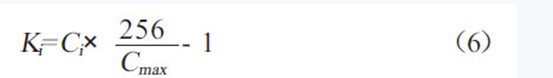
Where Cmax is the maximum gray value in each divided area, Ci is the maximum gray value of each corresponding area, and the calculated regional light control parameter Ki adjusts the output of the FPGA to adjust the brightness of the backlight, so that each of the corrected The RGB values ​​of the pixels are:
As shown in the scheme diagram, the line output from the controller, the field sync signal, and the corrected RGB signal are finally transmitted to the LCD panel.
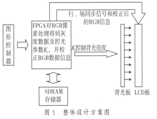
The main functions of SDRAM in the scheme are two: one is to store the line, field synchronization information and RGB data information transmitted from the graphics controller when the FPGA processing is not timely; the second is to store the data processed by the FPGA. , the information that the single LCD board can handle in the future. The purpose of this design is to achieve the effect that data is not lost and information transmission is more timely.
2 drive circuit design
In the choice of driver chip, we use TI's TLC5947, each channel is modulated by 12bits PWM pulse width, with 24 output channels, so a data transfer cycle will receive 288bits of data. The required voltage of the chip is 3.0 ~ 5.5V, there is a temperature control system, when the temperature of the chip is too high, it will automatically disconnect to protect the chip.
As can be seen from pin 25 of the chip, this chip supports cascading and can work with multiple chips to drive a larger display screen. From pin 1 to pin 24, each output channel is controlled by 12-bit input data. The internal contains a 4MHz crystal oscillator. The ratio of the input data to 212 or 4,096 is the duty cycle of the output pulse, thus achieving the corresponding backlight. PWM modulation of the area. It can be seen that TLC5947 divides the gray level into 4,096 levels, and we can subdivide the brightness of the backlight with large scale and precision to achieve better dynamic backlight effect.

The resistance in the driver circuit is determined by the current of the LED being driven. For details, refer to the TLC5947 configuration table (as shown in Table 1). The chip has strict timing requirements for the input SCLK, XLAT, BLANK and other signals. The capacitance between the power supply and the ground mainly plays a filtering role, and the value is selected as large as possible.
Table 1 Configuring the relationship between resistance and drive current
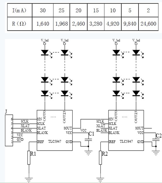
Figure 3 backlight drive circuit
3 software design
The control signal for this chip is supplied by Altera's development board model EP1C3T144C8 with a crystal oscillator of 50MHz.
From the experimental results, the data transmission mechanism of the chip is: every transmission cycle, every 1 S rising edge will read 1bit data from the SIN port into the register, which will be read in the falling edge of SCLK. Data is transmitted from SOUT (internal data is still reserved) and is lost to the next level until 288 bits of data are read. Each group of 12bits is sent to its own channel, and each group of data is read first in the higher order, and then arranged in order. For example, the read data is arranged in time order, 1, 0, 0, 0, 0, 0, 0, 0, 0, 0, 0, 0, then the corresponding control signal is 100000000000, then the duty cycle of the control channel That is:
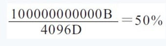
According to the principle that the PWM modulation area is equal, the effective voltage is about half of the supplied voltage.
According to the requirements of the simulation conditions, the SCLK clock signal needs to be low for a period of time every time 288bits is received, and the timing requirements of the chip are met as much as possible. In addition, the control signal BLANK needs to have a high-level conversion when each cycle is idle (when no data is transmitted), so that the data in the latch can be cleared to accept a new round of control data, otherwise, the lamp The brightness is obviously darker.
The RGB data is processed by the FPGA, converted to the corresponding gray value, and then the corresponding light control parameter Ki is calculated (we can divide the gray level by no more than 4,096), and transmitted to the SIN of the TLC5947, which can realize dynamic backlight adjustment. .

4 Conclusion
Through theoretical analysis and experimental testing, the dynamic backlight adjustment control system has done a good job in energy saving and image display contrast, which is very good in energy saving and emission reduction, building a harmonious society and the future development of LCD displays. Application prospects.
Figure 7 shows the dynamic backlight adjustment effect obtained by FPGA control and image pixel control. It can be seen that if the LCD backlight is used, the brightness of all backlight LEDs will be the brightest (lower right corner). ) Consistent, and now we divide it into different regions, so that each region has its own optimal brightness, without having to use the brightest of the entire image as a standard, and does not affect the display. In this way, we achieve the purpose of the dynamic adjustment we expected.
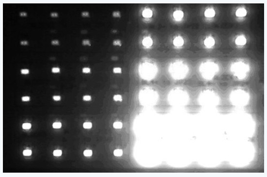
Figure 7 backlight renderings
Edit: Nizi
Military battery has a wide application on some high-tech euquipment including military communications equipment, submarine, drone , warship, government and so on .
The design for Military Battery Pack is more strict than normal lithium or Lipo Battery packs ,because it must meet some tough requirements as ;
1, high-level safety : military Lithium Battery was demanded to provide high-level safety and will not cause any death or accident with High intensity impact and and hit.
2, high reliability: the Military Battery must be reliable and could not causing any problems to the equipments during operating .
3, High environmental adaptability: the military Battery Pack is demanded to use in different temperature ,air pressure and other enviornmental condition.

Military Batteries : Ni-Mh Battery Pack BB-390/U
Besides ,the military always have a strict standard on low power self-consuming and deep life cycles .so these above standard has made it special from the other Lithium Battery Pack or other battery packs which applied to life .
Military Batteries
Military Batteries,Military Battery,Military Vehicle Battery,Military Solar Battery
YFJ TECHNOLOGY (HK) CO.,LIMITED , http://www.yfjpower.com