
1 Introduction With the increasing application of digital technology, ASIC [2] devices represented by Field Programmable Gate Array (FPGA) [1] have been rapidly popularized and developed, and the integration and speed of devices are both Growing at a high speed. FPGAs combine the high logic density and high reliability of gate arrays with the user programmability of programmable logic devices, reducing the risk of system design and maintenance, reducing product cost and shortening design cycles.
This article refers to the address: http://
At present, the rapid development of signal processing technology, communication technology and multimedia technology has benefited from the wide application of DSP [3] technology. But for portable and home voice systems, designs based on general DSP chips are not ideal. First of all, the chip cost and development cost of DSP are still relatively high at this stage, especially the cost of the chip, which is far less than the cost of high-volume ASIC chips. Secondly, portable devices are very demanding in size, which limits the use of some DSP chips, and volume is one of the advantages of ASIC chips.
This paper presents a hardware circuit implementation scheme of an FPGA-based audio processing chip. Due to the improved algorithm of the FIR filter, the size of the chip is greatly reduced and the power consumption of the chip is reduced.
2 Algorithm research and improvement
2.1 Ordinary FIR Filtering Algorithm The Nth-order FIR filter can be represented by the following linear convolution: [4] 
x(n) is the input audio sequence, and y(n) is the filtered audio sequence, and h(k) is the coefficient of the Nth-order filter.
Simply implementing this algorithm requires N+1 multiplications and N additions. So at least one hardware multiplier and a fixed point or floating point adder are needed to implement this function. Since the audio processing chip only needs to do linear convolution, we do not need to adopt the structure of the multiplier. In general, due to the large structure of the multiplier, it takes up most of the area on the chip and consumes most of the power. A structure that does not use a multiplier will save considerable chip area and power consumption. In order to achieve this structure, we need to improve the FIR filtering algorithm.
2.2 Improved Filtering Algorithm First, the filtered coefficient h(k) is expressed in binary notation (POT, Power of Two):
For example: h(k)=0.1172=2-3-2-7-2-16
We give a set of coefficients for the 7th-order filter, expressed in POT (accuracy less than 10-4):
h(0) = 0.3761 = 2-1-2-3+2-10+2-13-2-15
h(1) = 0.3083 = 2-2+2-4-2-8-2-12
h(2) = -0.9424*10-1 = -2-3+2-5-2-11
h(3) = 0.6439*10-1 = 2-4+2-9-2-14
h(4) = -0.3308*10-1 = -2-5-2-9+2-13
h(5) = 0.1663*10-1 = 2-6+2-10+2-15
h(6) = -0.4135*10-2 = -2-8-2-12+2-16
h(7) = 0.1877*10-2 = 2-9-2-14-2-16
The output value y of the filter when n=7 is as follows:
y = (2-1-2-3+2-10+2-13-2-15) * x(7)
+(2-2+2-4-2-8-2-12) * x(6)
+(-2-3+2-5-2-11) * x(5)
+(2-4+2-9-2-14) * x(4)
+(-2-5-2-9+2-13) * x(3)
+(2-6+2-10+2-15) * x(2)
+(-2-8-2-12+2-16) * x(1)
+(2-9-2-14-2-16) * x(0)
Obviously, the coefficients of x(n) are all 2 negative k powers, so we can combine x(n) with the same coefficients.
y(n)=2-1(...2-1(2-1(2-1u1+u2)+u3)+...)+u16)
Uj=xj(1)+ xj(2)+......+ xj(rj)
Where 1 ≤ j ≤ 16, xj(i) ∈ {x(nk)}, 1 ≤ i ≤ rj
From the previous coefficients, you can get:
U1 = x(n-6)-x(n-7); U2 = -x(n)+x(n-5);
U3 = -x(n-3)-x(n-7); U4 = x(n)+x(n-4);
U5 = -x(n-1)-x(n-6); U6 = -x(n-2);
U7 = x(n)+x(n-5); U8 = x(n-3)-x(n-4)+x(n-7);
U5 = -x(n-1)-x(n-6); U10 = 0;
U11 = x(n-5); U12 = x(n-2)-x(n-4);
U13 = x(n-1)+x(n-3); U14 = -x(n)-x(n-2);
U15 = x(n-1); U16 = x(n);
According to this algorithm, first find the value of U1, then shift the result to the right by one, then add the result to the value of U2, and so on, you can get y(n). We use a number of additions and 16 shift operations to complete the FIR filtering, and the complexity and power consumption of the algorithm are greatly reduced.
3 audio processing chip design
3.1 Structure Overview In the structure of the entire audio processing chip, we did not use any multiplier, but instead an adder and shifter. The result of the adder is output to the shifter, and the output of the shifter is fed back to the input of the adder, and the loop operation implements the function of the filter.
Considering the 7th-order FIR filter, you need to sample x times 8 times, so the input data should be stored in an 8*16 DataRAM (16-bit sampling accuracy). The size of the coefficient RAM (ProgramRAM) depends on the number of operations. In the above mentioned algorithm, there are 28 operations, so the size of ProgramRAM cannot be less than 28. Here we use a 32*6 ProgramRAM to satisfy The algorithm needs.
Considering the scalability of the audio processing chip, we set an EEPROM outside the audio processing chip to store the coefficients. When the chip is started, the data is transferred from the EEPROM to the ProgramRAM to adapt to the coefficients of different FIR filters. The programmability of the audio processing chip is greatly enhanced.
The modules of the audio processing chip mainly include EEPROM, ProgramRAM, DataRAM, serial-to-parallel conversion module, parallel-to-serial conversion module, address generation module, and main controller module.
3.2 Addressing Mode Description When the system is started, the additional EEPROM stores the system parameter values, including the address value of the input signal in the DataRAM and the corresponding flag bit (32*6bit), which are sequentially read into the ProgramRAM.

Among them, Zero, Sign, Shift are the operation control
Zero means no operands
Sign means adding a negative operand
Shift indicates shift operation
Virtual Address represents the virtual address of the operand.
The Base Address always points to the address of the earliest written value in DataRAM, that is, the address of x(n-7), and the other values ​​of Virtual Address are relative to the address of x(n-7), so the operand can be obtained. The actual address in DataRAM:
Physical Address=BaseAddress+VirtualAddress
Take u1 in y(n)=2-1(...2-1(2-1(2-1u1+u2)+u3)+...)+u16) as an example
U1 = x(n-6) - x(n-7);
Parameter setting: C1= x(n-6)=000001
C2=-x(n-7)=011000
※The lowest three digits represent the storage address
※ The 4th bit indicates the shift flag, and C2(4) is 1 means that the U1 is calculated to be shifted to the right and 2-1* U1 is calculated.
※ The fifth digit indicates the sign bit and controls the addition and subtraction. C1(5) is 0 for addition, and C2(5) is 1 for subtraction.
※The highest position, that is, the sixth position is 1 when Un=0, here only C19(6) is 1
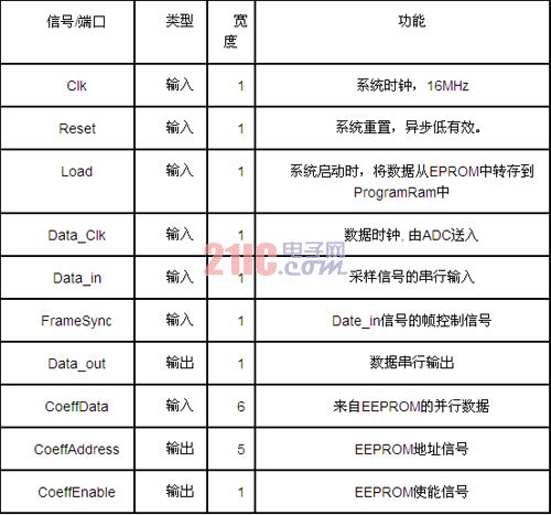
3.3 Port Description
3.4 Module design
3.4.1 EEPROM [5]
· EEPROM is used to store system parameters
· EEPROM is a 32*6bit storage array
· The input to the EEPROM is Enable, Address (4 downto 0)
The output of the EEPROM is CoeffData (5 downto 0)
The first unit of the EEPROM stores the number of operations; for example, the first unit stores "011100" to indicate that there are 28 operations in total.
3.4.2 ProgramRAM [6]
ProgramRAM receives system parameters in EEPROM
ProgramRAM is a 32*6bit storage array
The input of ProgramRAM is Write, Read, DataIn (5 downto 0), Address (4 downto 0)
The output of ProgramRAM is Zero, Sign, Shift, DataAddr (2 downto 0)
3.4.3 Serial to Parallel Conversion Module [7] (Serial2Parallel)
Serial2Parallel receives serial data, data clock and frame sync signals from the ADC
Serial2Parallel converts serial input signals into 16-bit parallel signals
The input of Serial2Parallel is DataClk, DataIn, FrameSync
The output of Serial2Parallel is DataOut (15 downto 0), DataOutSync
3.4.4 parallel and serial conversion output module [7] (Parallel2Serial)
Parallel2Serial converts parallel signals into serial signals
The input to Parallel2Serial is DataIn (15 downto 0), DataClk, FrameSync
The output of Parallel2Serial is DataOut
3.4.5 Main Controller Module (Main Controller)
The main controller module is the core of the entire design, which coordinates the work of the other modules.
· The main controller module is a state machine designed according to the operation flow chart
3.4.6 Address Generation Module (AddressGen)
PhysicalAddress is actually an adder that adds VirtualAddress to BaseAddress to generate a read address.
BaseAddress is actually a counter, and the IncreaseBase signal control is incremented by one to generate a write address.
MUX selects the read address or writes the address to the DataRAM
4 audio processing chip simulation
4.1 Simulation Waveform
4.2 Simulation Results Through the program, a set of input sequences were compared with the simulation results. The results obtained are shown in Table 1.
Table 1: Comparison of simulation results 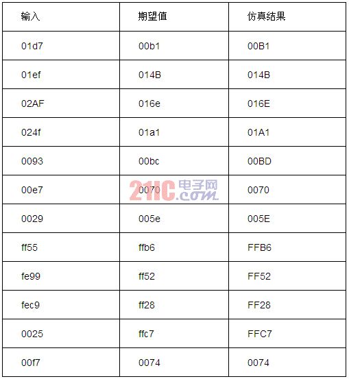
It can be seen from Table 1 that the audio processing chip has achieved the expected design goals and the effect is good.
It can be seen that the expected value and the simulation result will have an error of ±1 on the last bit, which is because the shift algorithm we use will not round off the last displacement. After calculation, this error does not affect the accuracy of the FIR.
5 Conclusion The audio processing chip designed in this paper mainly implements the FIR filter function, which can meet the needs of relatively simple voice signal processing. The POT coefficient representation method is used to represent the system parameters, and the multiplier function is implemented by an adder and a shift register, so that there is a considerable advantage in area power consumption. The design process uses a top-down design approach. The final simulation results meet the expected requirements
This brush is Small Turbo Brush. It's a specil Vacuum Cleaner brush. It's a good helper of acarus killing,so it will give you a safe and clean environment. It's mainly made up of multi-function soft brush,colorful pneumatic brush body,transparency cover and rotation type brushing fur. It's also a vacuum cleaner brush with six functions. First,automatic compensation function into the wind that will let rolling brush always run. Second,unique and simple structure, tear open outfit clean is very convenient. Third,high efficiency of dust collection and super silent. Fourth,deep cleaning and professional in addition to mites. Fifth,modelling is novel and beautiful. The last one is its new function that is rotating transformation multifunctional suction brush. This is really a very useful and beautiful vacuum cleaner brush,hope you will like it. Now let's see picture blow.

Small Turbo Brush
Small Turbo Brush, Turbo Brush, Vacuum Turbo Brush
Ningbo ChinaClean Household Appliances Manufacture Co., Ltd. , http://www.chinaclean-elec.com