
Electromagnetic interference is generated by an interference source, which is an electromagnetic phenomenon that is external and detrimental to the useful signal. The electromagnetic energy generated by the electromagnetic interference source is transmitted to the sensitive device through a certain transmission route, and the sensitive device exhibits some form of "response" to this, and produces the "effect" of the interference, the action process and the result thereof, For electromagnetic interference effects. In people's lives, electromagnetic interference effects are widespread and vary in form. If the interference effect is very serious and the equipment or system fails, resulting in a serious fault or accident, this is called an electromagnetic compatibility fault. Obviously, electromagnetic interference has become a huge obstacle that must be overcome on the road of modern electronic technology development. In order to ensure the normal operation of electronic systems or equipment, it is necessary to study electromagnetic interference, analyze and predict interference, limit the intensity of human interference, study effective technical means to suppress interference, improve anti-interference ability, and rationalize the electromagnetic environment.
Modern electronic products are becoming more and more powerful, electronic circuits are becoming more and more complex, and electromagnetic interference (EMI) and electromagnetic compatibility issues have become major problems. Advanced computer-aided design (CAD) greatly expands the ability of circuit design in electronic circuit design, but it has limited help for electromagnetic compatibility design.
At present, EMC has basically set up corresponding market access certifications in various regions of the world to protect the electromagnetic environment of the region and the competitive advantages of local products. Such as: North American FCC, NEBC certification, EU CE certification, Japan's VCCEI certification, Australia's C-TICK certification, Taiwan's BSMI certification, China's 3C certification are all "passports" to enter these markets.
1 Electromagnetic compatibility problem
Electromagnetic compatibility design is actually designed to optimize the electromagnetic interference generated in electronic products, making it a product that meets the electromagnetic compatibility standards of various countries or regions. The definition of EMC is: in the same electromagnetic environment, the device can not work normally due to the interference of other devices, and does not affect the interference of other devices.
Typical electronic circuits are made up of resistors, capacitors, inductors, transformers, active devices, and wires. When a voltage is present in the circuit, an electric field is generated around all of the live components. When a current flows through the circuit, a magnetic field is present around all of the carrier fluid.
A capacitor is the most concentrated component of an electric field. The current flowing through the capacitor is the displacement current. This displacement current is due to the fact that the two plates of the capacitor are charged and an electric field is generated between the two plates. By the electric field induction, the two plates generate charge and discharge to form a displacement current. In fact, the current in the capacitor circuit does not actually flow through the capacitor, but only charges and discharges the capacitor. When the two plates of the capacitor are opened, the two plates can be regarded as a set of electric field radiating antennas, and the circuit between the two plates will induce an electric field between the plates. The circuit between the two plates is either closed or open. When the direction of the electric field changes continuously, a displacement current is generated in the conductor in the same direction as the electric field.
The electric field strength is defined as the potential gradient, that is, the ratio of the potential difference to the distance between two points. A wire that is several meters long, when it flows through a few amperes of current, the voltage across it is at most a few tenths of volts, that is, the electric field strength of several tens of millivolts per meter, which can generate several amps of current in the conductor. . It can be seen that the electric field is effective and its interference ability is strong.
Inductors and transformers are the most concentrated components of the magnetic field, and the current flowing through the secondary winding of the transformer is the induced current. This induced current is generated by magnetic induction when a current flows through the primary coil of the transformer. The circuit around the inductor and the transformer can be seen as an induction coil of a transformer. When the magnetic lines of force generated by the leakage inductance of the inductor and the transformer pass through a circuit, the circuit generates an induced current as a "secondary coil" of the transformer. The circuit of two adjacent loops can also regard one of the loops as the "primary coil" of the transformer, and the other loop can be regarded as the "secondary coil" of the transformer, so two adjacent loops are also produced. Electromagnetic induction, that is, mutual interference.
As long as an electric field or a magnetic field exists in the electronic circuit, electromagnetic interference occurs. In high-speed PCB and system design, high-frequency signal lines, integrated circuit pins, various types of connectors, etc. may become radiation interference sources with antenna characteristics, which can emit electromagnetic waves and affect other systems or other subsystems in the system. normal work.
2 EMC design of the power supply
At present, most electronic products are powered by switching power supplies to save energy and improve work efficiency. At the same time, more and more products also contain digital circuits to provide more application functions. Switching power supply circuits and clock circuits in digital circuits are the most important sources of electromagnetic interference in electronic products. They are the main content of electromagnetic compatibility design. The following is an analysis of the electromagnetic compatibility design process of a switching power supply.
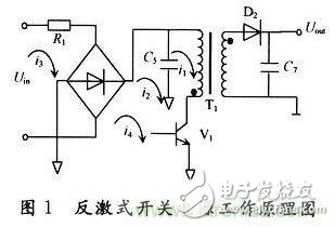
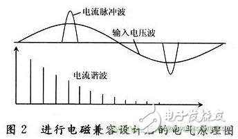
Figure 1 is a schematic diagram of a commonly used flyback or flyback switching power supply. The 50 Hz or 60 Hz AC grid voltage is first rectified by the rectification stack and charged to the energy storage filter capacitor C5 and then to the transformer T1. It is powered by a load circuit composed of a switching tube V1. Figure 2 is an electrical schematic diagram of an EMC design.
(1) Suppression of current harmonics. Generally, the capacity of the capacitor C5 is large, and the voltage ripple at both ends is small, about 10% of the input voltage, and the rectifier diode is turned on only when the input voltage Uin is greater than the voltage across the capacitor C5.
Therefore, during one cycle of the input voltage, the conduction time of the rectifier diode is short, that is, the conduction angle is small.
A pulse spike current will appear in the rectifier circuit as shown in Figure 3.
Such a pulse spike current, as developed with a Fourier series, is considered to consist of a very large number of higher harmonic currents that will reduce the efficiency of the power supply, ie, the power factor is low and will be poured back to The power grid pollutes the power grid. When it is serious, it will also cause fluctuations in the grid frequency, that is, the AC power supply flickers. Pulse current harmonics and AC power flicker test standards are: IEC61000-3-2 and IEC61000-3 -3. The upper limit of the general test pulse current harmonic is the 40th harmonic frequency.
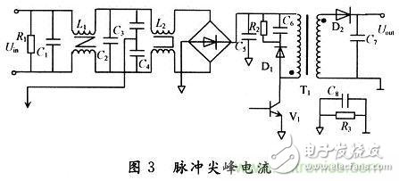
To solve the problem of excessive pulse spike current in the rectifier circuit, a power factor correction (PFC) circuit or a differential mode filter inductor is connected in series in the rectifier circuit. The PFC circuit is generally a parallel type step-up switching power supply, and its output voltage is generally 400 V DC. The power factor is not only 0.4 to 0.6, and the power factor is generally up to 0.4 to 0.6. 0.98. Although the PFC circuit can solve the problem of excessive pulse spike current in the rectifier circuit, it will bring about new high-frequency interference problems, which also requires strict EMC design. Differential mode filter inductors can effectively suppress the peak value of the pulse current, thereby reducing current harmonic interference, but can not improve the power factor.
L1 in Fig. 2 is a differential mode filter inductor, and a differential mode filter inductor is generally made of a silicon steel sheet material to increase the inductance, in order to prevent magnetic saturation when a large current flows through the differential mode filter inductor. Generally, the two sets of coils of the differential mode filter inductor each have a leakage magnetic circuit. The L1 differential mode filter inductor can be obtained according to the test or calculated according to the following formula:
E=Ldi/dt
Where: E is the difference between the input voltage Uin and the voltage across the capacitor C5, that is, the voltage drop across L1, L is the inductance, and di/dt is the current rise rate. Obviously, the smaller the current rise rate is required, the greater the inductance is required.
(2) Suppression of the ringing voltage. Since the primary leakage of the transformer has a sense of leakage, when the power switch V1 is turned from saturation to off, a back electromotive force is generated. The back electromotive force charges and discharges the distributed capacitance of the primary coil of the transformer, thereby generating a damped oscillation, that is, generating a vibration. Bell, as shown in Figure 4.
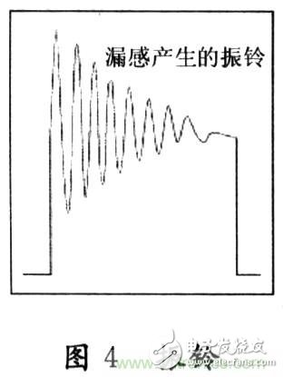
The voltage amplitude of the primary leakage inductance of the transformer is generally high, and its energy is also very large. If no protective measures are taken, the back electromotive force generally breaks down the power switch tube, and the damped oscillation generated by the back electromotive force is also strong. The electromagnetic radiation not only causes serious interference to the machine itself, but also causes serious electromagnetic interference to the surrounding environment of the machine.
D1, R2, and C6 in Fig. 2 are effective circuits for suppressing the back electromotive force and the ringing voltage amplitude. When the primary leakage inductance of the transformer generates a counter electromotive force, the counter electromotive force charges the capacitor C6 through the diode D1, which is equivalent to the capacitor absorbing the back electromotive force. Energy, which reduces the magnitude of the back EMF and ringing voltage. After the capacitor C6 is fully charged, it will discharge through R2, and correctly select the time constant of the RC discharge, so that the remaining voltage of the capacitor is exactly equal to the square wave voltage amplitude when the capacitor is next charged. At this time, the power supply has the highest working efficiency.
(3) Suppression of conducted interference signals. In Figure 1, when the power switch tube V1 is turned on or off, a pulsating DC i1 is generated in the circuit composed of the capacitor C5, the primary of the transformer T1, and the power switch tube V1, if the current loop is regarded as a transformer " Primary coil". Due to the high rate of change of current i1, the electromagnetic induction generated in the "primary coil" also induces electromagnetic induction to the surrounding circuits. The surrounding circuits can be regarded as multiple "secondary coils" of the same transformer, and the leakage inductance of the transformer T1 also induces the respective "secondary coils". Therefore, the current i1 is induced by electromagnetic induction, and the induced currents generated in each "secondary coil" are respectively referred to as i2, i3, ..., in. Among them, i2 and i3 are differential mode interference signals, which can be transmitted to other lines of the power grid through two power lines and interfere with other electronic devices. I4 is a common mode interference signal, which is generated by a circuit composed of other circuits of electromagnetic induction and earth or casing, and other circuits are connected with the earth or the casing through capacitive coupling, and the common mode interference signal can pass. Power lines and ground are conducted into other lines of the grid and interfere with other electronic equipment.
The circuit connected to the collector of the power switch tube V1 is also the main cause of the common mode interference signal. Because in the whole switching power supply circuit, the potential of the collector of the digital power switch V1 is the highest, up to 600 V or more, and the potential of other circuits is lower than this, so the collector of the power switch V1 and other circuits (including the power supply) There is a strong electric field between the leads of the input end. Under the action of the electric field, the circuit generates a displacement current, which is basically a common mode interference signal.
Capacitors C1, C2 and differential mode inductor L1 in Figure 2 have a strong rejection of the differential mode interference signals of i1, i2 and i3. Since C1 and C2 are also charged when the power cord is pulled out, it is easy to get an electric shock, so a discharge resistor R1 should be connected to both ends of the power input.
It is generally difficult to completely suppress the common mode interference signal i4, especially in the case of no metal casing shielding, because in the circuit that induces the common mode interference signal, one of the "components" is the circuit board and the earth. The equivalent capacitance between the "components" is generally unstable, and the design should have sufficient margin for the indicator. In Figure 2, L2 and C3, C4 are common mode interference signal suppression circuit devices. In the circuit with large input power, L2 generally uses two or even three, one of which is mostly a toroidal core inductance.
According to the above analysis, the main cause of electromagnetic interference is the main circuit through which i1 flows. This circuit is mainly composed of capacitor C5, transformer T1 primary and power switch tube V1. According to the principle of electromagnetic induction, the induced electromotive force generated by this loop is:
e=dφ/dt=SdB/dt
Where: e is the induced electromotive force; φ is the magnetic flux; S is the area of ​​the current loop; B is the magnetic induction intensity, and its value is proportional to the current intensity; dφ/dt is the flux change rate. It can be seen that the induced electromotive force is proportional to the area of ​​the current loop. Therefore, to reduce electromagnetic interference, we must first try to reduce the area of ​​the current loop, especially the loop area through which the i1 current flows. In addition, in order to reduce the influence of the leakage inductance of the transformer on the electromagnetic induction of the surrounding circuits, on the one hand, it is required to reduce the leakage inductance of the transformer; on the other hand, a thin copper sheath is wrapped around the periphery of the transformer to form a low-impedance short-circuit coil. The induced energy generated by the leakage current is consumed by the eddy current.
(4) Suppression of radiated interference signals. Electromagnetic radiation interference is also generated by electromagnetic induction, which is generated by a charged body or a current loop and a magnetic induction loop. Any one conductor can be regarded as an electromagnetic induction antenna. Any current loop can be regarded as a loop antenna. The leakage inductance of the inductor coil and transformer is also an important component of electromagnetic induction radiation. It is impossible to completely suppress electromagnetic radiation, but by properly designing the circuit or taking partial shielding measures, the electromagnetic interference radiation can be greatly reduced.
For example, minimizing the length of the circuit leads and reducing the area of ​​the current loop is an effective way to reduce electromagnetic radiation; correctly use the energy storage filter capacitors and install the energy storage filter capacitors as close as possible to the ends of the active device power leads. Each active device is powered independently or separately by a storage filter capacitor (a fully charged capacitor can be considered as a separate power supply) to prevent active devices (amplifiers) in each circuit from being generated through the power and ground lines. Crosstalk; strictly separating the ground of the power lead from the ground of the signal source, or adopting a two-wire parallel centering crossover method for the signal leads, so that the interference signals cancel each other out, which is also an effective method for reducing electromagnetic radiation; The electromagnetic interference can be partially shielded, and the signal lead can also be parallel shielded by the double ground, so that the signal line is sandwiched between two parallel ground lines, which is equivalent to the double loop, and the interference signals will cancel each other, and the shielding effect Very significant; the use of metal casings for machines or sensitive devices is the best way to shield electromagnetic interference, but non-metallic enclosures can also be sprayed Electrical materials such as graphite are shielded by electromagnetic interference.
(5) Elimination of high voltage static electricity. In Figure 1, if the output voltage is higher than 1 000 V, static elimination must be considered. Although most of the switching power supplies are transformers for "hot and cold" isolation, because of the "hot ground", also called "primary ground", the circuit can form a loop, and when the human body touches the "primary ground", it will "electric shock". Therefore, people call the "primary land" "hot place", meaning that they cannot be touched. "Cold land" is also called "secondary land". Although the voltage is very high, it does not form a loop with the earth. When the human body touches the "secondary ground", it does not "electric shock". Therefore, people all put "secondary" The land is called "cold land" and means that it can be touched. But whether it is "cold ground" or "hot land", its potential difference to the earth cannot be zero, that is, it will still be charged. For example, in a color TV set switching power supply, the "thermal ground" potential difference to the earth has a peak-to-peak value of about 400 V; the "cold ground" potential difference to the earth has a peak-to-peak value of about 1 500 V.
It is better to understand that "hot land" is charged, and it is difficult to understand that "cold ground" is charged. The "cold ground" charging voltage is generated by the secondary of the transformer. Although one end of the transformer secondary is connected to "cold ground", the true zero potential is in the center of the secondary winding of the transformer, or in the middle of the rectified output filter capacitor medium. This is called the "floating ground" of the power supply, ie it is zero potential but not connected to the earth. It can be seen that the voltage of "cold ground" is exactly equal to 50% of the output voltage. For example, the high voltage anode of the TV picture tube needs a high voltage of about 30 000 V. The true zero potential is between the high voltage filter capacitor (the graphite layer between the tubes). In the middle of the capacitor, or at the center tap of the high voltage package, the electrostatic voltage between the cold ground and the ground in the TV set can be determined to be approximately 15 000 V. Similarly, the "floating ground" of the "hot earth" loop is in the middle of the energy storage filter capacitor C5, so under normal circumstances the "hot ground" charging voltage is 50% of the rectified output, and its peak value is about 200 V. The counter electromotive force generated when the switch is turned on or off is also superimposed on it, and its peak-to-peak value is about 400 V.
R3 in Figure 2 is used to reduce the electrostatic voltage between "cold ground" and the earth. The role of C8 is to reduce the dynamic resistance between cold and hot ground. Generally, the digital circuit IC has a low withstand voltage. If the voltage of the "cold ground" is high, it is easy to break down the IC through electrostatic induction or human touch. The common EMC standards are as follows:
EMC universal series standard: IEC61000-4-X;   
General standard for industrial environmental immunity: EN50082-2;   
Pulse current harmonic test standard: IEC61000-3-2;   
AC power flashing test standard: IEC61000-3-3.
R3 in Figure 3 is used to reduce the electrostatic voltage between the cold ground and the earth. The role of C8 is to reduce the dynamic resistance between hot and cold ground. Generally, the digital circuit IC has a low withstand voltage. If the voltage of the "cold ground" is high, it is easy to break down the IC through electrostatic induction or human touch.
3 Conclusion
As the switching power supply continues to develop at high frequencies, its anti-interference problem becomes more and more important. In the development and design of switching power supply, how to effectively suppress the electromagnetic interference of the switching power supply, and improve the anti-interference ability of the switching power supply itself to electromagnetic interference is an important issue. In the anti-jamming design, several anti-interference measures are independent and related to each other, and various measures must be taken at the same time to achieve good anti-interference effect.
The telecom parts are metal or plastic equipment which is used for the purposes of telecommunication, like as telecom equipments and IT hardware: LSA Module, Krone Module, Disconnection Module, Distribution box, Label holder, Test plug, Wiring block, Rack screws
When you buy from Uonicore Electronics, you get quality telecoms equipment, good lead times, original parts and continued support for legacy equipment. In addition, you can support your environmental credentials with our recycling options and use of refurbished equipment.
Telecom Parts,telecommunication parts,telecom components,Server Rack Mount Screws
NINGBO UONICORE ELECTRONICS CO., LTD , https://www.uonicore.com