
Low-power system design requires attention to many non-traditional factors, from silicon process technology to software running on a microcontroller embedded platform. Careful examination at the system level reveals three main parameters that determine the power efficiency of the microcontroller: active mode power consumption; standby power consumption; and duty cycle, which determines the ratio of time spent on the two states, and this The ratio depends on the behavior of the software.
A low-power standby state can make a microcontroller seem very energy efficient, but its final performance can only be demonstrated by considering all the factors that affect active power.
A low-power standby state can make a microcontroller seem very energy efficient, but its final performance can only be demonstrated by considering all the factors that affect active power. For this and other reasons, the trade-off between process technology, IC architecture, and software architecture is some decision-making problem with some subtle and sometimes unpredictable results. The way in which the various functional blocks in an MCU are combined with each other has a significant impact on the overall energy efficiency. Even seemingly minor changes in hardware implementation can cause large fluctuations in total energy consumption over the life of a system.
Low-power applications
For example, meter reading and alarm systems usually have a battery for 10 years. A small increase in the read power consumption of a sensor (which occurs hundreds of millions of times during the life of the product) may reduce the actual field life of the product by several years. A simple smoke alarm that detects soot particles in the air every second and completes 315 million reads in its life cycle.
The activity ratio (or duty cycle) of a simple smoke alarm is also relatively low. Each sensor reading can take less than a few hundred milliseconds to complete, most of the time being spent on calibrating and stabilizing the MCU when waking up the ADC and other sensitive analog components to achieve a stable operating point. In this case, the duty cycle is the key to the design, which is inactive for about 99.88% of the time.
Traditional smoke alarms are relatively simple. Consider a more complex RF design with a sensor grid that forwards the readings to a master application. The sensor needs to listen to activity from a primary node, so that it can advertise that it is still in the mesh network or send the most recently captured information to the router. However, increasing activity may not affect the entire work cycle; instead, with higher performance devices, more functionality can be done during each activation. Due to the more advanced architecture and semiconductor technology, the increase in processing speed is possible, faster devices can provide higher energy efficiency, while slower devices run longer periods. The focus is on understanding the interaction between process technology, MCU architecture, and software implementation.
Silicon selection
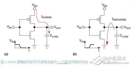
CMOS energy consumption data. Almost all MCU implementations use CMOS technology (Figure 1). The power dissipation of any active logic circuit can be expressed by the formula CV2f, where C is the total capacitance of the switching circuit path within the device, V is the supply voltage, and f is the operating frequency. Both voltage and capacitance are factors in the process technology used. Over the past three decades, CMOS logic's chip operating voltage has dropped from 12V to less than 2V due to the shrinking transistor size. Since the voltage is a quadratic term in the formula for active power consumption, the voltage drop has a significant effect.
Although the capacitance term is linear, the reduction of Moore's Law is also very beneficial to reduce its overall level. For a given logic function, a more advanced process provides lower capacitance, resulting in lower power consumption than the previous generation. In addition, advanced design techniques enable clock gating so that only the circuits that perform the actual task work, reducing the overall switching frequency.
Compared to other technologies, CMOS significantly reduces wasted energy; however, leakage current still exists. In contrast to active power dissipation, leakage power increases as Moore's Law scales down, and its considerations should be considered in any low-power application because most systems are inactive for a low duty cycle system. . But for active power, the circuit design has an important impact on the actual leakage. Similar to clock gating, power gating can greatly improve the effects of leakage, making more advanced process nodes a better choice for low duty cycle systems, although theoretically older process technologies can provide lower leakage values.
Suitable process technology. There is an appropriate process technique for each set of features. The answer is not simply dependent on a process technology with the lowest theoretical leakage value, because the device spends a lot of time in sleep mode. In sleep mode, most of the power in the MCU can be turned off and the leaked components removed from the formula. Leakage is a big problem when the circuit is active, but the advantage of advanced transistors is that they can be switched with much higher efficiency, which can easily offset this problem.
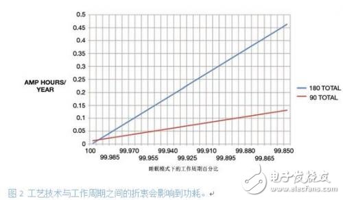
For example, the leakage current of the 90 nm process is about five times higher than the dedicated low power 180 nm process. Active mode power consumption is four times lower, but its base is a much larger value.
For example, a 180 nm MCU with an active power consumption of 40 mA and a deep sleep mode consumes 60 nA. Compared to these power levels, the power level achieved at 90 nm can reduce the active power consumption to 10 mA, but sleep. The mode current is high, 300 nA. For a 90 nm implementation, the MCU must be active for 0.0008% of the time to achieve higher overall energy efficiency. In other words, if the system only works for 1 second per day, the 90 nm version is about 1.5 times more energy efficient than its 180 nm counterpart. The conclusion is that when choosing a process scale, the key is to understand the application's duty cycle (Figure 2).
Once the right work technology is selected, IC designers can choose to further optimize energy performance. When clock gating was first introduced, it was only used at a relatively coarse level. Clock gating adds to the complexity of a system because the circuit designer needs to know which logic path requires a clock signal at any given time.
Clock distribution. Most MCU implementations use a hierarchical structure that distributes the clock signal and corresponding voltage levels to various parts of the IC. Each functional unit (such as instruction processing blocks and peripherals) is divided into groups, each group feeding a separate clock tree and power network. A divider or multiplexer obtains each set of clock signals from a common clock source. Similarly, if these groups require different voltages (which are becoming more common), then a set of power transistors and regulators will supply voltage to each set of peripherals.
To minimize the complexity of the design, the MCU uses a relatively simple clock gating method that shuts down the entire clock tree as long as none of the power items in a group are active. However, this method will clock the logic that does not work in the active group. For example, if the current instruction is a branch instruction, the addition unit in the CPU core will also receive a clock. As mentioned earlier, the conversion of the clock signal in the adder will increase the power consumption by 2 times CV.
Advances in design tools and techniques have enabled the granularity of clock gating to be increased to a point where the peripheral clock signal is not received if the peripheral or power unit does not operate during that period.
Voltage scaling provides a further potential for energy savings by providing a lower voltage for a specific set of functional units when necessary. The key to providing the proper voltage for a group of power cells or peripherals is the implementation of an on-chip voltage regulator or dc/dc converter, and the use of supervisory circuitry to ensure that the IC operates at the required voltage.
Power considerations. On-chip voltage regulators give system designers more flexibility to extract more power from a single battery. For example, an on-chip switching buck converter (such as Silicon Labs' SiM3L1xx MCU) can get input from a 3.6V industrial battery and convert it to 1.2V with more than 80% efficiency. Many MCUs do not have this feature. Instead, the linear components are stepped down to the appropriate level, which is a significant drain. In advanced implementations, the buck regulator can be turned off when the battery is discharged to a certain level and the converter is unable to do the conversion. As a result, the power supply optimizes energy efficiency throughout the life of the device, all under software control.
Parking Lot Lighting Led,Parking Lot Lights Waterproof,Led Parking Lot Ligh,Led Flood Light For Parking Lot
Vietnam JJ Lighting Company , https://www.vnjjlighting.com