Single-layer self-capacitance sensing technology will become the new layout focus of in-cell touch panel manufacturers. In order to improve the yield of In-cell touch panels, reduce costs and noise, the supply chain industry is planning to replace the existing two-layer mutual capacitance sensing technology with single-layer self-capacitance, including Apple, Samsung, and Taiwan. / Japanese panel manufacturers and first-line touch IC manufacturers have launched patent layouts and have invested in the development of new-generation touch ICs and liquid crystal display (LCD) driver ICs to improve the design structure of the In-cell sensing layer.

Li Xiangyu, general manager of Inventive Elements, believes that for panel makers, the process complexity of the self-capacitance In-cell structure is relatively low, and as long as the corresponding touch IC is available, mass production can be successfully launched.
Li Xiangyu, general manager of the invention element, said that In-cell touch will undoubtedly bring more imagination for the thin and light design of mobile devices, but the direct introduction of touch sensing layer (Rx) and driver layer (Tx) directly in the LCD will cause a lot of confusion Information, increasing the difficulty of panel and touch IC design; therefore, the technology is still limited by low process yield and high cost, delaying market penetration. This is to drive the touch panel manufacturers and the touch IC manufacturers to join forces to actively develop mass-produced In-cell touch technology.
Li Xiangyu pointed out that there is currently a consensus in the industry to abandon the In-cell design to detect changes in mutual capacitance between the sensing layer and the driving layer, and switch to a single-layer self-capacitance sensing method that directly introduces Vcom electrode lines into the sensing layer. On the one hand, it allows the touch panel factory to omit the manufacturing process of the metal bridge that isolates the sensing and driving layers, improves the process yield, and reduces the cost by 20-30%; on the other hand, it solves the problem of mutual capacitance interference caused by the close proximity of the two layers. Improve touch response speed and sensitivity.
In fact, self-capacitance technology has been in use for many years, but in the past, it could only collect the horizontal or vertical touch signals of the touch panel, support single-finger or two-finger touch functions, and it is prone to false touch (ghost point) problems. ; Therefore, under the development trend of multi-touch function, it is not popular for the mutual capacitance scheme that can accurately sense the intersection of the horizontal and vertical planes. However, after entering the era of In-cell, the noise problem of mutual capacitance is even more headache, so the industry has turned to the development of self-capacitance multi-touch, in order to further build the next generation of In-cell touch panels.
At this stage, in addition to Samsung ’s most active investment, most of the In-cell touch panel factories also have patent research; and SynapTIcs, Cypress, Duntai Technology and Inventive Elements and other chips Or silicon intellectual property (IP) developers, are fully deploying related touch IC solutions. Li Xiangyu believes that the entire industry chain has begun to focus on the operation structure of self-capacitance, which shows that this technology is extremely forward-looking in the field of In-cell applications.
However, the self-capacitance sensing layer provides touch signal generation, acquisition and driving functions. Initially, panel manufacturers had to thicken the ITO layer and increase the number of metal wires in the horizontal and vertical planes. They also required strict requirements for touch IC performance and signal noise. Ratio (SNR) and firmware function specifications can solve the problems of multi-point signal sensing and high resistance, which will increase the material cost and affect the transmittance of the panel. In addition, the LCD driver IC must also have a time-sharing processing mechanism and expand the buffer memory (Buffer) capacity in order to process In-cell touch and LCD signals simultaneously.
Li Xiangyu does not deny that the threshold of single-layer self-capacitance In-cell touch technology is extremely high, and it still needs a long time to develop. As a result, hybrid On-cell and In-cell bonding solutions began to gain attention, such as Sony ’s hybrid In-cell structure with the sensing layer above the upper glass and the driving layer introduced into the LCD. Due to the distance between the two layers Far mutual interference is less, so it can reduce the difficulty of touch IC development; the current yield rate of panel mass production has also reached as high as 80% to 90%, and the cost is declining fast. .
![]()
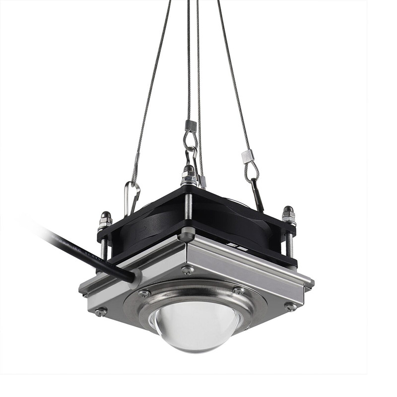
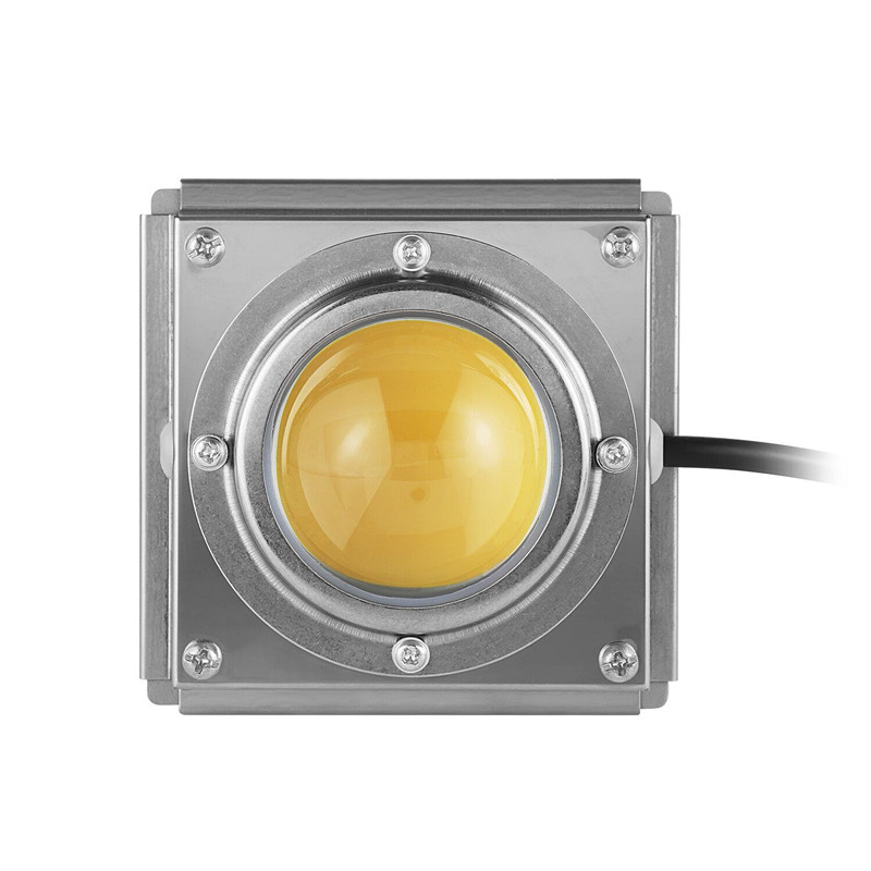
2020 Hottest Cob Grow Light diy model, 200w grow light , cob grow light, high power grow light, etc.
Can also do OEM/ODM service, More cob Led Grow Lamp is a great ideal for all kinds of indoor garden plants: lettuce, orchid, organic herbs, pepper, strawberries, succulent, hydroponic, medical plants.
Whether it's hydroponics, plants in soil, you can add a touch of magic to every veg and flower with Xeccon grow lights.


Cob Grow Light,Best Cob Led Grow Light ,Grow Light Cob Diy,Diy Grow Light
Shenzhen Wenyi Lighting Technology Co., Ltd , https://www.wycngrow.com
