
1 Introduction
LED is a kind of green illumination light source, its main advantage is high luminous efficiency. With the progress of material science, its luminous efficiency will be more greatly improved in the next ten years; and the energy consumption is low, the life is long, the material can be recycled, and it will not pollute the environment.
Based on the above advantages of LED lighting, Europe, America, Japan and South Korea have formulated corresponding laws and regulations and industrial support policies to promote related technologies to the field of civilian lighting on a large scale in the next ten years. Although China started late, it has also begun active research and development, industrial policy formulation and support in recent years.
2 High-power white LED street lamp luminous board design related application technology
At present, there are three main types of white LED technology: using InGaN blue LED die with a small amount of yttrium aluminum garnet as the main phosphor, the blue LED excites the phosphor to emit yellow light, and mixed with blue light to emit white light; using the principle of three primary colors Red, green, and blue LEDs are mixed into white light; ultraviolet LEDs are used to excite three primary color phosphors to produce multi-color light mixed into white light.
Among them, the second scheme is difficult to control, and it is difficult to ensure that the array application emits uniform white light. The white light emitted by the third white light technology has an ultraviolet component. Therefore, the first white light technology is selected for application technology analysis. The success of the invention of high-power white LEDs has provided material and technical guarantee for the entry of semiconductor light-emitting elements into the field of lighting. The use of high-power white light-emitting diodes in the field of lighting needs to pay attention to two aspects: electrical / optical conversion rate and thermal control of light-emitting components.
High-power LED is a small device. With the improvement of manufacturing technology, the input drive current is getting larger and larger, and the input power is also increasing. Although the electric / optical conversion rate is high, in terms of chip area, it should be counted as a point light source, so the heat generated per unit area is very large. The performance of high-power LED devices will be greatly affected as the junction temperature increases. After a certain temperature is exceeded, the electrical / optical conversion rate will drop sharply, and even the device will permanently lose its function because the temperature is too high.
2. 1 Chip-level application technology to improve the power / light conversion rate of high-power LED chips and make the heat flux density of the chips uniform
With the development of technology, the two-dimensional size of LED chips is continuously increasing. By expanding the area of ​​LED chips, the output power of LEDs is increased, and the luminous brightness can be greatly improved. However, if the chip area is increased blindly, adverse light phenomena such as an increase in the light absorption ratio inside the LED and a decrease in external quantum efficiency will occur, and the temperature rise of the junction temperature will further increase. Moreover, as the two-dimensional size of the chip increases, the luminous efficiency of the chip itself also drops rapidly.
In order to optimize the thermal and optical performance of the LED chip, on the one hand, in addition to increasing the size of the chip, on the other hand, by optimizing the electrode structure on the chip, the current of the entire chip during operation can be evenly distributed. If the current distribution is not uniform, it will often result in uneven distribution of heat flux density and luminous flux, and generate local hot spots inside the chip, which will greatly reduce the efficiency and reliability of the LED device.
To reduce the uneven distribution of lateral current in the LED chip, the effective current path length must be short and equal, and the length depends on the spatial distance between the positive electrode and the negative electrode. Fig. 1 (b) The chip electrode has a better uniformity of current density distribution in the whole chip after optimization than Fig. 1 (a).
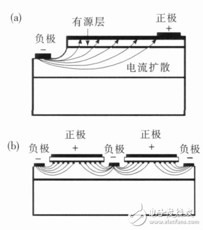
Figure 1 Current spread distribution of different electrode structures in LED
It can be seen that for large-chip LEDs, a single electrode design is not conducive to current diffusion, so the current high-power LEDs mostly use comb-shaped strip-shaped cross electrodes, comb-shaped strip-shaped and dot-shaped electrodes, and a rice-shaped electrode structure design. This can make the current distribution in the chip more uniform, make the light-emitting chip from a single-electrode point light source into a surface light source, improve the total light output flux of the chip, and can make the surface heat distribution of the chip uniform and prevent the occurrence of hot spots. Figure 2 shows a schematic diagram of the electrode structure of a mainstream high-power LED, in which the chip designed with a rice-shaped electrode is a patented product of the American Cree company.
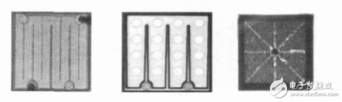
Figure 2 High-power LED chip electrode structure.
The main application of the M-shaped electrode structure is LEDs grown on a conductive silicon carbide (SiC) substrate, and the current is vertically diffused, compared to the lateral diffusion of LED chips with GaN-based comb electrodes grown on an insulating transparent sapphire (sapphire) substrate. Current, its current distribution is more uniform.
2. 2 Comprehensive application of high-power white LED in the packaging stage to extract light from the LED chip, ensure the quality of white light and rapid heat dissipation of the device
The crystal bonding stage: the LED chip is soldered and fixed on a thermally conductive substrate (heat sink), and an insulating layer, a circuit layer, and a reflective layer are generally coated on the substrate from bottom to top. Figures 3 to 5 show the three ways of soldering and fixing the chip on the substrate.
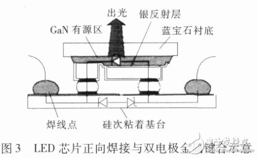
Figure 3 LED chip forward welding and dual electrode metal bonding schematic
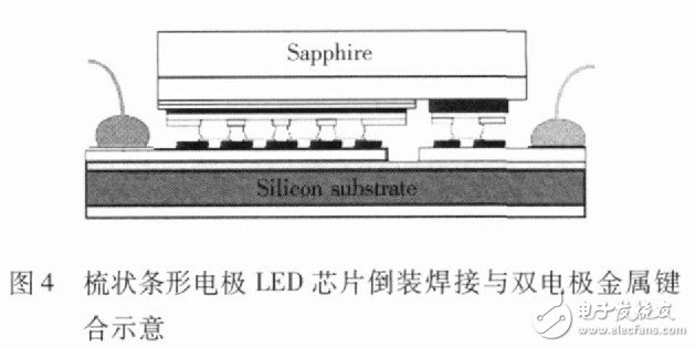
Figure 4 Comb strip electrode LED chip flip chip welding and dual electrode metal bonding schematic
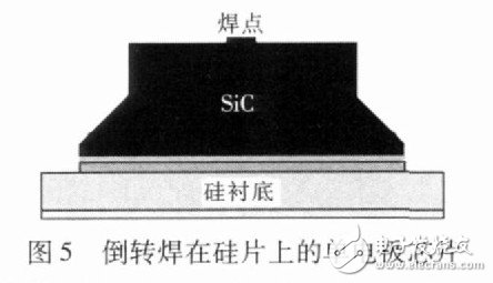
Figure 5 Single-electrode chip reversely soldered on a silicon wafer
Compared with the conventional LED chip of FIG. 3, the solid crystal method of FIG. 4 and FIG. 5 directly contacts the heat end of the chip with the heat sink layer, which is very easy to dissipate the heat. Considering the light extraction rate and heat dissipation, this is the current mainstream high-power LED chip welding and fixing method.
Mounting the shell: The mounted shell is generally processed into a cone or parabolic reflector to increase the light output of the power LED. It belongs to the secondary light extraction technology and increases the light extraction rate of a single chip.
Accuracy:
±0.1℃ 35.5℃-42.0℃ (±0.2 ℉ 95.9℉-107.6℉)
±0.2℃ under 35.5℃ or above 42.0℃(±0.4℉ under 95.9℉)
Waterproof display screen
Easy carrying and use
Digital Temperature Gun,Mini Digital Thermometer,Digital Infrared Thermometer,Non Contact Digital Thermometer
Axiswell Technology Co., Ltd , https://www.medhealthycare.com