
1 Introduction
In order to further improve the robustness and stability of real-time tracking of fast moving targets in complex scenes in the actual combat environment, the author proposes to build a master-slave ultra-high-speed parallel with dual DSP and FPGA as the core. The design idea of ​​the processing system is studied, and a new flexible airborne real-time image tracking system based on dual DSP is researched and developed. On the one hand, the dual DSP architecture to achieve parallel partitioning of system tasks makes the system extremely high processing speed; on the other hand, the introduction of field programmable logic device FPGA has greatly improved the flexibility of the system. The combination of the two can make the system fully reflect the characteristics of a new generation of on-board real-time image tracking system that is faster, more accurate and more flexible.
2 Dual DSP high-speed signal processing system features
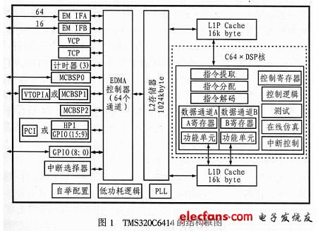
Texas Instruments (TI) introduced a new generation of digital signal processor TMS320C6414 (hereinafter referred to as C6414) with a frequency of 400MHz ~ 700MHz, its data processing capacity is 3200MIPS ~ 5760MIPS. The block diagram of the device is shown in Figure 1. Its main features are as follows:
(1) The DSP core adopts a very long instruction word (VLIW) architecture, which has 8 functional units and 64 32-bit general-purpose registers. It can execute 8 instructions simultaneously in one clock cycle, and the computing power can reach 5760 MIPS.
(2) In order to make the data meet the requirements of ultra-high-speed DSP core, C6414 adopts two-level cache, namely 16k Byte first-level data cache, 16k Byte first-level program cache and 1024k Byte data and program unified memory. .
(3) Added direct processing of packed data instructions to establish a seamless data stream to improve the efficiency of the instruction set;
(4) Each functional unit adds additional functions to the hardware, thereby enhancing the orthogonality of the instruction set.
3 system hardware design
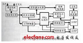
The hardware platform of the photoelectric imaging tracking system consists of six parts: image acquisition and preprocessing module, synchronous separation module, FPGA logic control module, dual DSP + dual port RAM image processing module, asynchronous communication module and graphic display module. The system block diagram is shown in 2. It can be known from Fig. 2 that the analog video signal output by the infrared detector and the visible light camera is introduced by the multi-channel signal selection chip, and after being pre-processed by clamping, amplification, filtering and desynchronization, the A/D converter will be used. The analog video is converted into an 8-bit digital signal and imported into the off-chip video buffers 1, 2, and then waits for the FPGA timing control DSP external interrupt to move all the cached data to the Level 2 cache in the DSP chip, and then realizes data reorganization through system task division. Then, synchronous parallel data processing is performed in the master-slave DSP, and the intermediate result is synthesized by the main DSP, and finally the final matching result is obtained after the subsequent operations are completed. At the same time, the main DSP transmits the target matching position information to the outside world by writing the graphic display buffer; the other analog signal is first introduced into the synchronous separator, and then the line sync signal is extracted and sent to the FPGA as a time base to generate the timing of the system. Control signal; the third analog signal is sent to the graphic superposition circuit as one of the input superimposed signals. When the field forward arrives, the FPGA interrupts control and reads the graphics memory data, and simultaneously implements the parallel/parallel data read in the FPGA chip. After the conversion, the output is shifted to the graphic superimposing circuit, and the two signals are sent to the video monitor to complete the graphic display on the video image. During the whole system operation, the main DSP also communicates with the external host computer through the asynchronous transceiver every 80ms, so that the system can receive external commands and target parameters in real time, and then adjust the working state of the tracking system.
3.1 Image Acquisition and Preprocessing Module
The multiplexer in this system uses the CD4052 chip. It can switch the infrared/visible video input according to different working situations; the video pre-processing circuit uses AD817 to amplify the video signal to obtain a clearer signal for video processing; the A/D chip selects AD9225 of AD company, the output is The 8bit digital video signal is sent to the 74LS245 for data latching.
3.2 Synchronous separation module
The system uses a dedicated video sync separator LM1881 to separate valid line/field sync signals from standard negative sync NTSC (PAL or SECAM) video signals and send them to the FPGA to generate various levels of logic control of the system. Output.
3.3 FPGA logic control module
Since the functions of each chip in the system are relatively independent, to coordinate the operation of these chips, a programmable chip with control logic is needed. For this reason, I chose ALTERAL's EPF10K30A, which has 246 user I/O ports. 30,000 typical gates, 216 logic array blocks, and 1728 logic units not only meet the control requirements of the system, but also provide control logic for future system expansion. In this photoelectric tracking system, FPGA is mainly used to complete the following aspects:
(1) Generate an A/D sampling control clock to achieve correct sampling of the analog video;
(2) providing a character graphics memory address and a chip select/read control signal, and controlling the reading of the graphic data when the field forward approach arrives;
(3) providing a video data buffer address and a chip select/write control signal to control continuous writing of the video data;
(4) generating external interrupt 4 to dual DSP, when the data fills the video image cache predetermined space, controlling the master-slave DSP to quickly move the data block to the on-chip level 2 cache;
(5) generating an external interrupt 7 to the main DSP, and controlling the main DSP to erase and write the character graphic memory data when the return time of each field comes;
(6) A parallel/serial conversion circuit is generated to serially shift the character pattern data read in parallel to the graphics superimposing circuit, thereby realizing superposition of "+" and "â–¡" graphics on the video image.
The internal structure block diagram of the FPGA is shown in Figure 3.
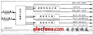
Figure 3 FPGA internal structure block diagram
3.4 Dual DSP + Dual Port RAM Image Processing Module
The high-speed parallel digital signal processing circuit uses dual DSP as the parallel processing core unit, and is supplemented by dual-port RAM to realize the video image cache, thereby completing the high-speed real-time target tracking processing task with large calculation amount. The composition and function of the parallel processing system are described as follows:
a. Video image cache submodule
In order to realize real-time image acquisition and high-speed processing, the system uses two dual-port RAMs to form independent video buffers, corresponding to the master/slave DSP processors. IDT's 3.3V asynchronous dual-port PRAM IDT70V657 is used in the design, and the ASRAM mode is adopted for the interface with the DSP. Since the EMIF ASRAM interface supports the 32Bit data interface, the use of the IDT70V657 to form an incomplete address structure to access data can better achieve the 8Bit latched data interface with the C6414 without the need to extend the width of the DPRAM. It also reduces the time overhead for the DSP to read external data.
The size of the IDT70V657 is 32K & TImes; the 36Bit system uses the way of dividing the two DPRAMs into two half fields before and after to realize the ping-pong switching when accessing data. That is, at any time during system operation, when data is written to the first half of the DPRAM, the data is read out to the DSP in the second half of the DPRAM. When the current half field is full of video data, the FPGA sends an interrupt signal to the DSP to inform the DSP to read the data written in the first half of the DPRAM, and at the same time, write the data of the A/D converter into the buffer space of the second half of the DPRAM, and so on. The data is read and written synchronously.
We are UV LED manufacturer from China.
5 years warranty
All of our product are meet with Reach, CE, RoSH, SGS, EN62471 standards.
We supply the safty UV LED. The peak wavelength range is between 365-430nm.

It is suitable for the application of electronic assembly, disinfection, beauty purpose, currency detection, medical and mosquito repelling.
We have use anti ultraviolet epoxy packag and high temperature resistant production technology in our products. In the past 18 years, we have been appreciated and recognized by our customers.
1, Variety of wavelength available:
365nm UV LED,370nm UV LED,375nm UV LED, 380nm UV LED, 385nm UV LED, 390nm UV LED, 395nm UV LED, 400nm UV LED, 405nm UV LED, 410nm UV LED, 415nm UV LED, 420nm UV LED, 425nm UV LED and 430nm UV LED.
2, Variety of power available: We can supply UV LED with 0.06W UV LED, 0.1W UV LED, 0.2W UV LED, 0.5W UV LED, 1W UV LED, 3W UV LED. We can also customized single chip UV LED, double chips UV LED, three chips UV LED or multi chip UV LED for you.
3, The length of pin: LED Lamp's pin can be 17mm, 29mm, 90 degrees bent feet, braided pin and so on. Tips: taping pins can operate on a robot, greatly improving the efficiency of manual plug-ins.
4, Multiple Shape/Size selection:
· Through-hole UV LED: 3mm round UV LED, 4mm round UV LED, 5mm round UV LED, 6mm round UV LED, 8mm round UV LED, 10mm round UV LED, 3mm flat top UV LED, 5mm flat top UV LED, 346 UV LED, 546 UV LED, 5mm Straw Hat UV LED, 8mm Straw Hat UV LED, 5mm short head UV LED, 3mm Short Head UV LED, 234mm Square UV LED, 255mm Square UV LED, 257mm Square UV LED.
· SMD UV LED: 2835 UV LED, 3528 UV LED, 3020 UV LED, 3014 UV LED, 3030 UV LED, 3535 UV LED, 5730 UV LED, 5050 UV LED, 2835 2-chip UV LED, 5050 3-chip UV LED ect.
5, Variety of angle available: 5 degree through-hole LED, 20 degree through-hole LED, 30 degree through-hole LED, 40 degree through-hole LED, 45 degree through-hole LED, 60 degree through-hole LED, 90 degree through-hole LED, 120 degree through-hole LED, 140 degree through-hole LED ect.
6, Colorful epoxy: Water clear, white diffused, pale white diffused.
We will do the High temperature resistance testing and 10 hours ageing treatment before the product out off the factory, which can ensure the stability of each product. Our LED products have 5 year warranty. Please believe that we are the best supplier for your light-emitting diode.
UV LED
UV LED, High Power UV LED, 365nm LED, UVA LED, 5MM UV LED, 1W UV LED
Shenzhen Best LED Opto-electronic Co.,Ltd , https://www.bestsmd.com