
Traditional integrated technologies are increasingly unable to meet the demands of today's very large and complex FPGA designs implemented at 90 nanometers and below. The problem is that traditional FPGA synthesis engines are based on ASIC-derived methods such as underlying planning, in-place optimization (IPO), and physically-aware synthesis. However, these integrated algorithms from ASICs do not apply to the general architecture of FPGAs and predefined routing resources.
This article refers to the address: http://
The end result is that all three traditional FPGA synthesis methods require multiple time-consuming design iterations between front-end synthesis and downstream place-and-route tools to achieve timing closure. The solution to this problem is a unique graphics-based physics synthesis that provides a one-pass, push-button operation that eliminates (or requires little) design iterations with downstream place-and-route engines. Moreover, graphics-based physical synthesis can increase performance by 5% to 20% in terms of overall clock speed. The Synplify Premier Advanced FPGA Physical Synthesis Tool is such a tool that is tailored for high-end FPGA design engineers with complex designs that require a true physical synthesis solution.
This paper first introduces the main traditional synthesis methods, and explains the related problems of these methods, then introduces the concept of physical synthesis based on graphics, and points out how this technology can meet the design requirements of current advanced FPGAs.
Problems with traditional integrated solutions
For the 2 micron ASIC technology node and before the early 1980s, the ratio of the delay associated with the circuit unit (logic gate) to the interconnect (connection line) related delay was about 80:20, which is the gate delay. It accounts for about 80% of each delay path. In this way, the designer can estimate the interconnect delay using the wired load model. In the wired load model, each logic gate input is assigned a “unit load†value, and the delay associated with a particular path. It can be calculated as a function of the strength of the drive gate and the total capacitive load on the connection.
Similarly, when the first RTL synthesis tool was used in ASIC design in the late 1980s (about 1 micron technology node), the delay of the circuit unit was still dominant compared to the connection delay. Status, the ratio is about 66:34. Therefore, early synthesis tools were based on their latency estimation methods and optimized using a simple wire-loading model. Since the delay of the circuit unit dominates, the timing estimation based on the wire load used by the initial synthesis engine is accurate enough, and the downstream place and route engine can usually be repeated in relatively few iterations (between the RTL and the synthesis phase) Implement the design below.
However, with the introduction of each subsequent technology node, the interconnect latency is greatly increased (in fact, the ratio of delays between circuit cells and interconnects is now close to the standard cell ASIC implemented in 2005 with 90 nanometer technology). 20:80). This makes the correlation between the delay estimate of the synthesis engine and the actual delay after placement and routing getting lower and lower.
This has some important implications because the synthesis engine chooses between different optimization methods and between alternative methods of implementing functions, such as adders based on their timing predictions. For example, suppose a particular timing path that contains an adder (and other components) is predicted to have some (timing) margin. In this case, the synthesis tool can choose a slower adder version that occupies a relatively small chip area. . However, if the timing estimate is significantly larger than the actual post-layout delay, the path may end up being very slow. In this way, the inaccurate delay estimation means that the synthesis engine finally optimizes the incorrect object. Only after the layout is completed, you find that the problem is not what you (or the synthesis engine) thinks. As a result, the amount of work required to achieve timing closure is greatly increased because the number of design iterations from front-end to back-end is greatly increased.
In order to solve these problems, it is necessary to understand the physical characteristics related to the design in the synthesis process. Therefore, over time, ASIC synthesis technology (following FPGA synthesis technology) has adopted a number of approaches (and in some cases abandoned some methods), such as the underlying planning, IPO, and physics-consciousness discussed below. Comprehensive.
Bottom planning
For the RTL synthesis of ASICs, the underlying planning techniques emerged in the early 1990s, a little later than the advent of integrated technology itself. The underlying planning tools allow designers to define physical areas on the device, lay them out by hand or using automated interaction techniques, and assign different parts of the design to those areas.
The underlying planning involves synthesizing and optimizing the design on a module-by-module basis, and then “stitching†everything together at the end (the integrated algorithms used in the early underlying planning tools are based on the connected-line load model). This means that the underlying planning tool cannot optimize the logic per unit and only affects the layout of the logic modules. Moreover, by definition, the underlying planning tool does not consider routing resources globally, and it is not possible to accurately analyze all timing paths until the design is fully wired. This can lead to a lot of time-consuming design iterations between front-end and back-end tools. Although this approach can improve the timing performance and power consumption of ASIC designs, it requires complex analysis of the design and a high level of expertise.
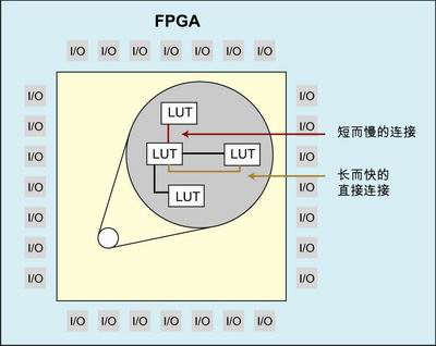
Figure 1: The mainstream architecture of the FPGA.
In the early days, there were several reasons for adopting ASIC underlying planning: to solve the problem of limited capacity as a way to obtain time convergence, and to support incremental changes on a module-by-module basis. Recently, the underlying plan is no longer considered a way to obtain timing closure itself; the underlying plan is still a useful method, but only useful when combined with other methods (such as physical optimization), using a synthetic backdoor The underlying planning of the level netlist still requires a lot of expertise.
For FPGAs, the underlying planning techniques were not mainstream until the late 1990s. On average, in an FPGA design, critical paths typically pass through three regions. Due to the design approach commonly used by FPGAs, if a comprehensive ("gate level") netlist is used to perform the underlying planning, even relatively small changes to the RTL may result in the previous underlying planning work being lost. The solution to this problem is to do the underlying planning at the RTL level. However, to be more useful, this must be combined with some form of physical optimization, and the physical synthesis algorithms derived from the ASIC are not suitable for the general architecture of the FPGA and the predefined routing resources.
Layout optimization
As the role of the underlying planning in the ASIC field weakened, IPO technology strengthened/replaced it in the mid-1990s. This again involves timing analysis and estimation based on the integration of the connection line load model.
In this case, the generated netlist is passed to the downstream place and route engine. After the place and route and parasitic extraction, the actual delay is backed up to the synthesis engine. These new value triggers are incrementally optimized in the synthesis engine, such as logical refactoring and replication. The result is a new netlist that has been partially modified. This netlist is then submitted to the incremental place and route engine, resulting in an improved design topology.
The final results based on the IPO process are generally better than those obtained using the underlying planning approach. However, this approach may also require many design iterations between the front-end and back-end tools. And an important issue based on the IPO approach is that modifications to the place and route may lead to new critical paths that were not visible in the previous iteration, ie fixing a problem may provoke other problems, which may result in Convergence problem.
For FPGA designs, the IPO-based design process began to receive mainstream attention in 2003. However, although such a process is already available, at the time these processes were not adopted in a meaningful way, because IPO techniques that individually optimize timing paths typically result in incomplete degradation of other path timings and incomplete timing closure. Designers need reliable results that allow them to make changes to the design without sacrificing the results of previous design releases. But IPO-based methods do not produce stable results over multiple design iterations, because optimizing critical paths in one iteration creates new critical paths in the next iteration. Similarly, increasing constraints to improve the timing of one region may degrade the timing of other regions.
Physically aware synthesis
&nbs
p; The current state-of-the-art ASIC synthesis technology is a combination of physical awareness, which began to receive mainstream attention in about 2000. Regardless of the actual technology (there are several different algorithms), the basic concept of physics-awareness is to combine layout and synthesis in a one-time process.
This works well in the ASIC world because the synthesis engine that understands the layout can estimate timing based on the perimeter of the placed cells and Steiner and Manhattan cabling estimates. The reason this integrated approach works well in ASICs is that the connections are arranged in an orderly fashion. This means that the delay associated with the final layout and layout design has a very good correlation with the results estimated by the synthesis engine.
From 2002 to 2003, many EDA vendors began to consider the application of physics-aware integrated technologies from ASICs to FPGA designs, but they did not further develop this idea, and Synplicity's new An exception to this is the graphical-based synthesis approach, where no vendor can provide layout-aware RTL synthesis tools for FPGA design. The problem is that unlike the "build in order" connection in the ASIC, the FPGA has a fixed number of predetermined routing resources, not all of the wiring is set to the same (some connections are short and fast, some are long And fast, some short and slow, some long and slow).
For practical situations, ASIC-based physics-integrated synthesis can be routed and timing estimated based on the proximity of the laid out cells that form the design. For FPGAs, placing two logical functions in adjacent areas does not necessarily achieve a fast connection between them. - Depending on the available routing resources, placing the connected logic function farther may result in better routing and timing results, although this is a bit counterintuitive. That's why the physics-inspired synthesis technology from ASIC design does not give the best results when used in an FPGA architecture. Similarly, the design flow using these techniques requires a lot of time-consuming design iterations between the front-end (synthesis) and back-end (layout and routing) engines to achieve correlation and timing closure.
Some considerations related to FPGA architecture
Before describing the concept of physics-based synthesis in detail, it is important to understand the complexity of design tasks. As mentioned earlier, FPGAs have fixed connection resources, all connections have been built, but not all paths are the same (short, medium, and long connections, and each connection is possible Has fast, medium or slow characteristics).
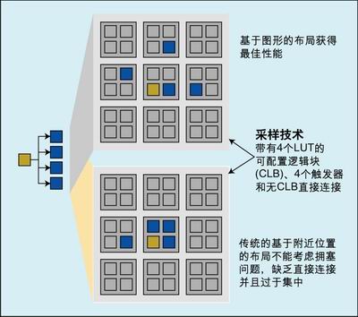
Figure 2: A more traditional and graphics-based layout.
Each path may have multiple "tap points" (like the exit path of a highway). The problem here is that you might have a fast path that quickly passes a signal from the source point function (the initial entrance of the highway) to a destination function (the last exit of the highway). However, if we add a second destination function to an internal tap point, this can greatly slow down the signal speed.
Moreover, the mainstream architecture of today's FPGAs is based on the concept that a lookup table (LUT) has several inputs and a single output. Some FPGA architectures have different delays for each input and output path associated with the lookup table. However, the more important fact is that each input to the LUT may only use a portion of the different wire types. If the output from one LUT drives another LUT, there may be both slow and fast paths between them, depending on the specific input we are using on the receiving LUT.
The overall situation is further complicated by the layering nature of the FPGA architecture. For example, a small logic module may have several LUTs; there are several such small modules in a larger logic module; there are a large number of such large logic blocks throughout the FPGA. In one of these large logic blocks, the probability that the output of one LUT is directly connected to the input of another LUT is small; in order to implement additional connections, it may be necessary to bypass the outside of the logic module and then wrap around The module is implemented internally. This again illustrates the complexity of the problem being handled: if you know where to place them and which pin to use, placing two objects/instances on different logic blocks will result in a non-optimal interconnection. A shorter delay will be obtained in the same module of the resource.
In addition, any proposed integrated solution must address the associated connection delays around fixed hard macro resources such as RAM, multipliers, and so on. Similarly, the solution must address increased routing congestion, which often occurs near these hard macros. All of these hard macros are part of a particular device, so any proposed solution must be available for each device in each FPGA family.
Graphic-based unique physical integration solution
A physically conscious integrated solution that truly addresses the complexity of the FPGA architecture will handle these issues from a completely different perspective. This approach describes the characteristics of all the wires in the FPGA, including entry points, endpoints, and internal exit points, and then builds a “map†for all of these wires. For the software industry, this type of map is called a graph; that's why this method is called "graphics-based physics synthesis."
In addition to the wiring itself, this graphic includes these details: which LUT pin is connected to which type of wire; the delay difference from the input to output of each LUT; and the size and location of any hard macros in the device. For example, this is similar to looking at the map to show the streets, highways, and places like parking lots (hard macros) that you will drive through. When you want to travel through two places in the city, you will use the map to choose the fastest path, which is usually not the shortest point-to-point path.
Similarly, the graphics-based physical synthesis engine does not look for the nearest path, but instead focuses on speed using an interconnect-centric approach. Start with the most critical path and then step to the next critical path (so that the most critical path gets the fastest route), the graphics-based physical synthesis engine will select the wires and their associated entry and exit points; These connections get the circuit layout; accurate delays are obtained from these connections and layouts; finally optimization and design iterations are performed as required.
The key point is that all optimizations and iterations are performed in the front-end part of the process (integrated). The graphics-based physical synthesis output is a fully laid-out netlist (including the specific LUT pins that will be associated with each wire) that can be passed to the FPGA's back-end place-and-route engine.
The result is a one-pass, push-to-button integration step that the downstream place and route engine does not require (or requires very little) design iterations. Moreover, based on an analysis of more than 200 actual designs, a graph-based physical synthesis can achieve a performance improvement of 5% to 20% in terms of overall system clock speed.
Summary of this article
In the ASIC-centric, physics-conscious synthesis, where the wires are derived from layout choices, when using graphics-based physics synthesis in FPGA design, the layout is derived from the choice of connection lines.
For timing closure problems, existing (from ASIC) physical synthesis engines may require many time-consuming design iterations between the front-end (synthesis) and back-end (layout and route) of the process. After all these iterations, they may still not converge. In comparison, analysis of more than 200 designs using graphics-based physics synthesis shows that 90% of the designs are within 10% of the final actual timing, and 80% of the designs are within 5% of the actual timing values. With a logic synthesis design of only 30% within 5% of the actual timing value, many design errors can easily reach 30% or even higher). Moreover, graphics-based physical synthesis can improve overall clock speed performance from 5% to 20%.
In addition, the quality of the graphically-based physical synthesis of the laid-out netlist is greatly improved, which means that the timing-driven routing tool has a small amount of work and optimizes execution, so that the operation will be very fast.
Synplicity's breakthrough is based on the concept of a wire-centric approach, as well as graphical representation of everything and then processing the graphics. After extensive research and development, Synplicity's comprehensive experts have created a true graphics-based physics integration solution. The first product with a graphical physics-integrated feature is Synplify Premier, an advanced FPGA physics synthesis tool designed for high-end FPGA designs that are complex in design and require a true physical synthesis solution. The Synplify Premier tool also includes advanced features such as RTL native debugging and support for the ASIC prototyping tool Synopsys DesignWare.
Small Electrical Connectors
Electronic Cables,Electrical Wiring Harness Co., Ltd. , http://www.nbwireharnesses.com