
In the world of mixed-signal simulation, many analog engineers find themselves struggling with understanding analog-to-digital converters (ADCs). Analog technology is widely regarded as one of the most challenging fields in electronics, and even experienced professionals often spend years mastering it through trial and error. For a junior analog engineer, the path to proficiency can seem daunting. This article aims to guide you by covering essential knowledge about ADCs, helping you build a solid foundation in analog technology.
What is an ADC and what does it stand for?
ADC stands for Analog-to-Digital Converter. It is a device that transforms continuous analog signals into discrete digital values. In other words, it converts real-world signals—like voltage levels from sensors—into a form that can be processed by digital systems.
How ADCs Work
An ADC typically performs four key steps during the conversion process: sampling, holding, quantization, and encoding.
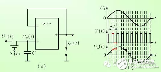
Sampling and Holding
The first step involves capturing the analog signal at specific intervals. The sampled value is then held constant to allow for accurate processing during the next stages.
Quantization and Encoding
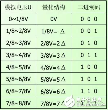
Once the signal is sampled, it is converted into a digital value. The smallest change in the digital output corresponds to one least significant bit (LSB), also known as the quantization unit (Δ). The process of assigning this value is called quantization. Finally, the result is encoded into a binary format, which becomes the output of the ADC.
Types of ADCs
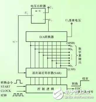
ADCs can be categorized based on their working principle, including flash (parallel), successive approximation, dual-slope, and counter types. One common type is the successive approximation ADC, which uses a comparator, a DAC, a successive approximation register (SAR), and control logic to determine the digital output.
Understanding the ADC0808/0809
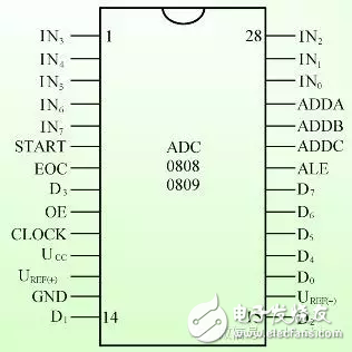
The ADC0808/0809 is an 8-bit ADC commonly used in various applications. It has several pins, such as IN0–IN7 for analog inputs, ADDA, ADDB, ADDC for channel selection, and D7–D0 for digital output. Other important pins include CLK (clock), ALE (address latch enable), START (start signal), EOC (end of conversion), OE (output enable), VCC, GND, and reference voltage pins UREF(+) and UREF(-).
Main Technical Parameters of ADCs
Resolution refers to the smallest change in input voltage that the ADC can detect, usually expressed in bits. Higher resolution means better accuracy. Quantization error is the difference between the actual analog value and its digital representation, typically less than or equal to 1 LSB. Accuracy includes both absolute and relative accuracy, where absolute accuracy measures the maximum deviation from ideal performance, while relative accuracy expresses this deviation as a percentage of the full-scale range.
Conversion time is the time required to complete an ADC cycle, from the start of the conversion to the availability of the digital output. These parameters are crucial when selecting an ADC for a specific application.
Key Performance Indicators and Common Misconceptions
When choosing ADC products, users often fall into certain misconceptions. For example, some believe that higher CPU count or faster clock speeds directly translate to better performance. However, these factors alone do not reflect the true capabilities of an ADC, especially since performance depends heavily on the system architecture and software optimization.
Other myths include overemphasizing memory size, number of ports, or switching capacity. These metrics may be relevant in other contexts like switches or servers, but they don't necessarily indicate the performance of an ADC. Instead, the key indicators for ADCs include layer 4/7 throughput, new connection rates per second (L4 CPS and L7 CPS), transaction rate (L7 RPS), concurrent session handling, and anti-DDoS capabilities.
It's important to understand how different manufacturers test and report these metrics. For instance, F5 provides multiple L7 CPS definitions, and the correct comparison should focus on the standard "L7 Connection per Sec (1-1)" metric rather than others that might inflate results.
Other metrics like SSL performance, DNS QPS, and HTTP compression are also relevant for specific use cases but are not part of the core ADC performance evaluation.
Conclusion
As an analog engineer, understanding ADCs is essential for designing and optimizing mixed-signal systems. By focusing on the right performance indicators and avoiding common misconceptions, you can make more informed decisions when selecting and using ADC components in your projects.
Antenk extended its connector product range by SD card connectors. As already mentioned there are various applications, in the past driven by the computer industry, which are using memory cards as well in their end products, single sided pressure contact connectors can be designed and manufactured according to a customer specific requirement based on customer dedicated insulator- and contact dies. Such single sided pressure contact connectors are mainly used as board to board connection on the base of direct contact to the pads on the board.
Compact Flash Card Connector Overview
Store More Memories
Compact Flash storage cards are small, removable, mass-storage devices. They electrically comply with Compact Flash Association standards, the PC Card ATA standard, and run in True IDE mode. These 50-position cards typically hold between 32 MB and 2 GB of memory and are about the size of a matchbook. Antenk`s connectors include headers that can accept Type I (3.3mm thick) or Type II (5.0mm thick) storage cards, flush and raised mounting heights, and ejectors. Antenk Compact Flash card connectors also provide electrostatic discharge protection.Adapter for Compact Flash Card type I and II
Available with various ejectors
Different stand offs heights
Reverse type without stand-off height is not applicable to Compact Flash Card Type II
Compact Flash Card Connector Specification
Insulation Resistance: 1000MΩ at 500V DC
Withstanding Voltage: 500Vrms
Current Rating: 1A AC/DC max.
Contact Resistance: 40mΩ max. at 20mV max.
Operating Temp. Range: -55°C to +85°C
Reflow Solder Temp.: 220°C min. / 60 sec, 260°C peak
Mating Cycles: 10,000 times
Materials and Finish
Insulator: LCP, glass filled (UL94V-0)
Push Button: Glass reinforced PBT (UL94V-0)
SMT Metal: Brass, pure Sn
Pivot Shell: Stainless Steal
Contacts: Brass
Plating: Contacts - Gold (15µ[) over Nickel (40µ[), Solder Tails - pure Sn
Compact Flash Card Connector Product Features
Compact Flash Connectors
Robust surface-mountable designs
Proven PCMCIA contact technology
Accepts hardware for mechanical mounting
Top- and bottom-mounting styles
Right-angle and vertical orientations
Compact Flash Connectors Applications
Desktop and laptop computers
Digital cameras
Smart phones
Data recorders
Slot machines
Industrial and embedded computers
SD Card Connector,Tf Card Connector,Sd Card Connectors,Natural Cf Card Connector,Compact Flash Card Connector,CF cards types I/II,CF Card connector MA type Adapter,CF Card connector MA type Ejector
ShenZhen Antenk Electronics Co,Ltd , https://www.antenk.com