
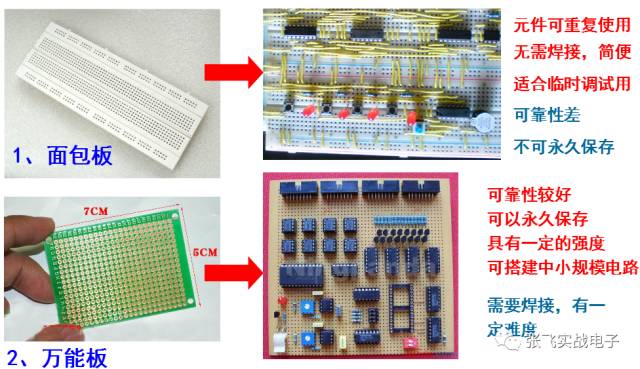
**Comparison of Advantages and Disadvantages Between Breadboard and Universal Board**
**Universal Board Soldering Methods**
When laying out components on a universal board, many people are used to the "top-down" approach, which involves placing key components like chips first and then connecting other parts based on their wiring. This method is planned during soldering, which makes the process more systematic and efficient. However, due to the lack of experience, beginners may find this challenging. It's better for beginners to sketch a layout on paper first, draw the component positions with a pencil on the front side of the board, and then plan the connections accordingly before starting to solder.
For the soldering technique on a universal board, flying wires are commonly used. While this method doesn't require much skill, it's important to keep the routing as horizontal and vertical as possible to make the layout clean and organized, as shown in the image below.
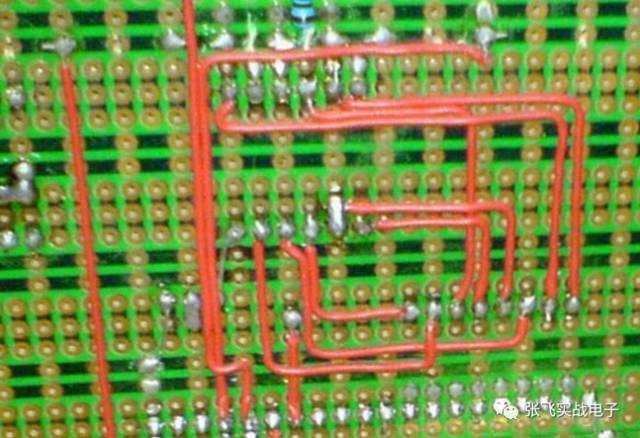
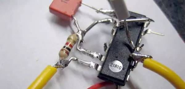
**Common Flying Wire Connection Method**
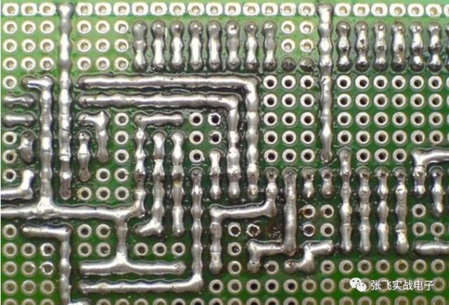
Another popular method online is the tin wire connection. As shown in the figure, this method offers good performance but uses a lot of tin. Pure tin wiring can be difficult, and it’s affected by factors such as the type of tin wire and the soldering technique. A simpler alternative is to first pull a thin copper wire and then use it to connect the required points. The soldering method on a perforated board is quite flexible, and each person can develop a style that suits them best.
**Universal Board Soldering Skills**
Many beginners struggle with unstable connections, leading to short circuits or open circuits. In addition to poor layout and bad soldering, lack of skill is a major cause of these issues. Mastering some techniques can greatly simplify the physical circuit, reduce the number of flying wires, and improve stability. Here are some tips from my own experience:
1. **Initially determine the layout of the power supply and ground wire**
The power supply runs through the entire circuit, and a well-planned layout plays a crucial role in simplifying the design. Some boards have copper foil running through specific holes, which can be used as power or ground lines. If not, you should plan the power and ground layout in advance.
2. **Be good at using the component pins**
When soldering a universal board, many jumpers and wires are needed. Don’t rush to cut off extra pins; sometimes, connecting directly through the component pins can be more effective. Also, leftover pin leads can be saved and reused as jumper wires.
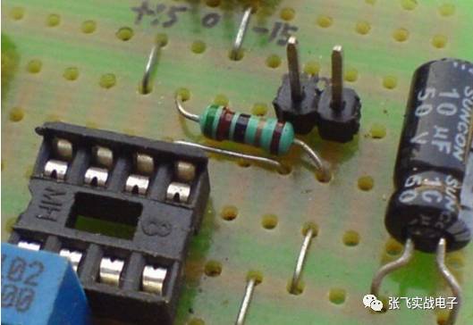
3. **Be good at setting jumpers**
Jumpers not only simplify the connections but also make the layout cleaner and more professional, as shown below.
4. **Be good at using the structure of the component itself**
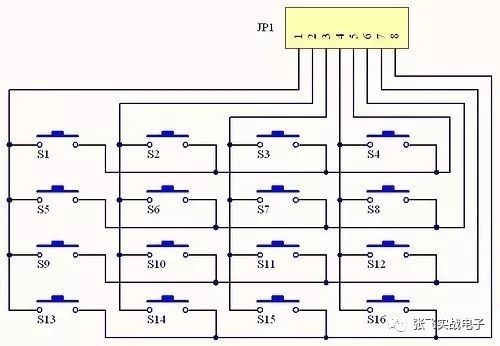
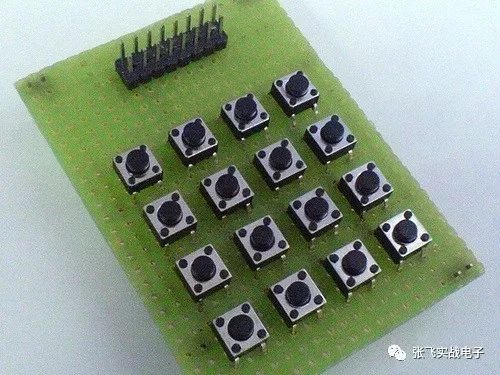
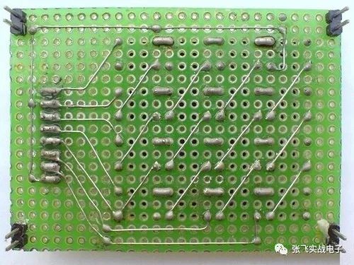
For example, in a matrix keyboard circuit, the buttons have four legs, two of which are connected. This feature can be used to simplify the wiring, as demonstrated in the following figures.

5. **Be good at using pin headers**
Pin headers are very versatile. They can serve as mechanical and electrical connections between two boards, similar to how computer boards are connected.
6. **Cut the copper foil when needed**
If space is limited, a small knife can be used to cut away unnecessary copper foil, allowing more components to fit in the same area.
7. **Make full use of the double panel**
Double-sided boards are more expensive, so it's important to take advantage of both sides. Each pad can act as a via, enabling flexible connections between the front and back.
8. **Make full use of the space on the board**
Components can be hidden inside chip holders, making the board look neater and protecting the components.
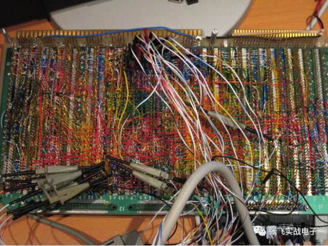
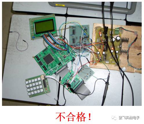
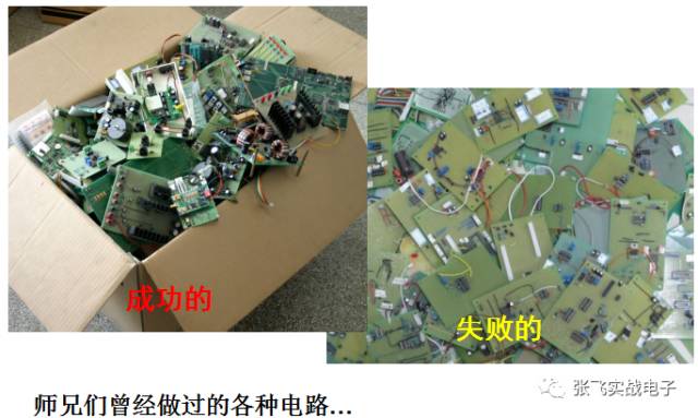
**The Rookie vs. the Veteran: A Contrast That Scared!**
The board made by a beginner might look like this:
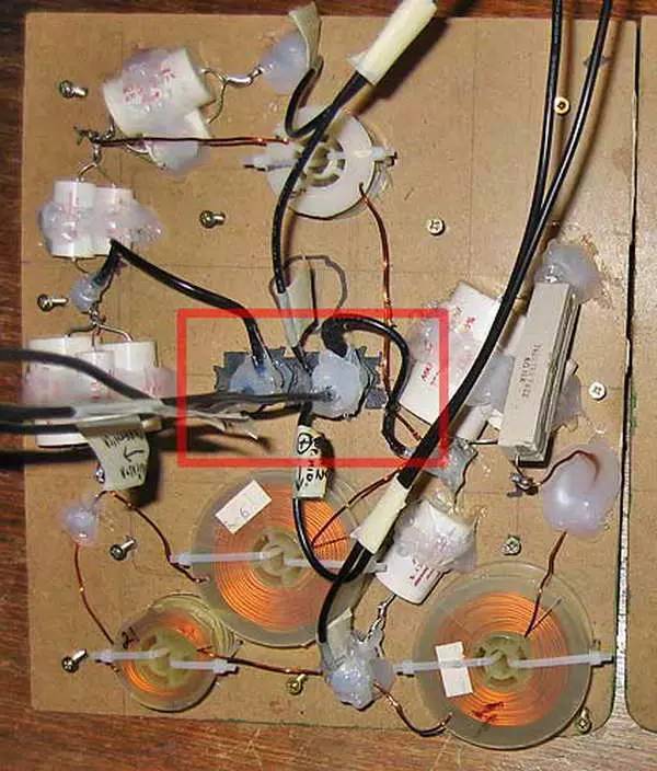
While a veteran’s board looks like this:
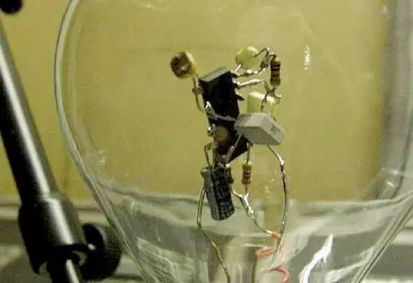
Of course, there are even those who can create beautiful designs without a board. Some can build complex circuits, and others even go as far as building a CPU using logic gates on a universal board — it’s just stunning!

**Let’s Talk About the Basic Steps and Methods of Building a Circuit with a Universal Board**
**First, Preparation Work**
1. **Schematic Drawing and Simulation**
Key points:
- Circuit block: Provide approximate partitioning of functions for layout and soldering.
- Parameters of key points (input, output, special points, etc.) provide theoretical values for debugging.
2. **Preparation of Components**
Key points:
- Check component values and labels carefully.
- Ensure all components and consumables are ready before starting.
- Test components before soldering whenever possible.
3. **Preparation of Tools**
A constant temperature soldering station is recommended for better control.
4. **Installation of Copper Posts**
Mounting copper posts at the four corners helps prevent accidental short circuits.
**Second, Pre-Layout**
1. **Arrange Important Components and Interface Devices**
Layout should be reasonable, compact, and easy to connect and solder.
2. **Consider the Signal Flow Direction**
Signals should flow in a clear direction to avoid crossing.
3. **Record Layout, Remove Components**
Use a pencil to mark the positions of key components and signal flow.
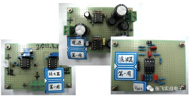
**Third, Build the Power Part**
1. **Build the Power Section**
Solder and test the power circuit first to ensure the whole system works properly.
2. **Build the Signal Processing Part**
Start from the signal source and build one module at a time, testing after each step.
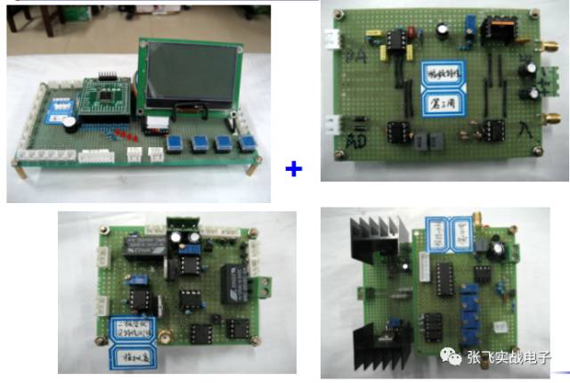
3. **Complete Soldering**
Inspect joints, fix any bad ones, and clean up messy wires.
4. **Overall Circuit Test**
Test functionality, indicators (like accuracy), and verify that it meets the design goals.
**Fourth, Data Organization**
1. **Draw a Formal Circuit Diagram**
- Note any changes and reflect them in the final diagram.
- Mark key test points.
2. **Test Report**
- Organize original data and create a form.
- Compare actual results with theoretical values.
- Confirm whether the design met its expected goals.
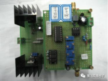
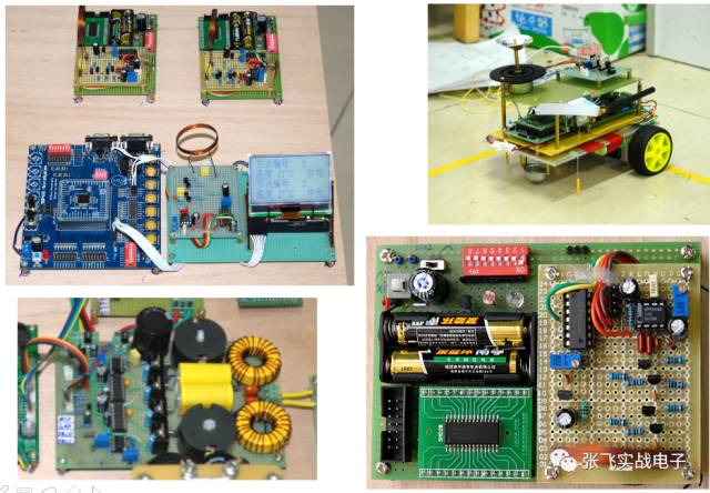
**Fifth, Qualified Circuit Construction Works**
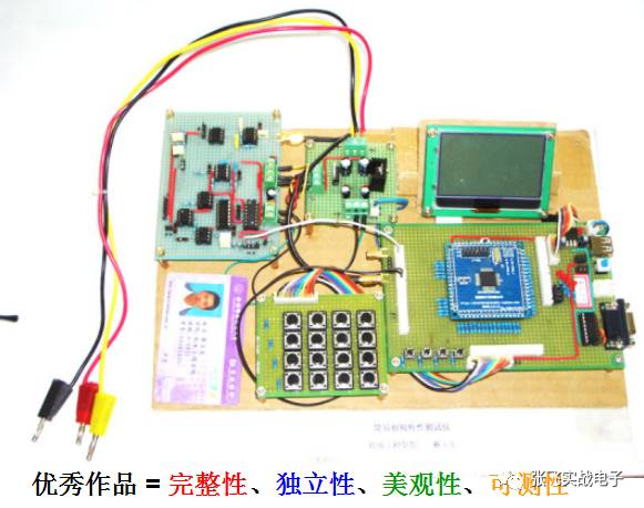
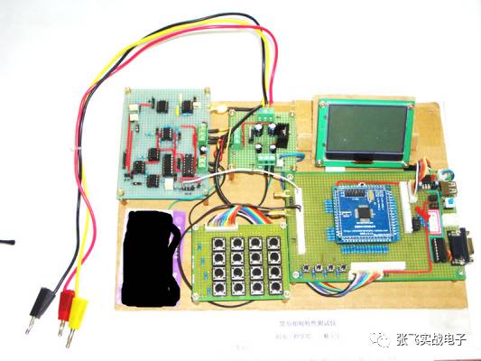
Excellent work = integrity, independence, aesthetics, and testability.
Zirconia Ceramics,Zirconia Engineering Components,Zirconia Precision Parts,Zirconia Wear Resistant Parts
Yixing Guanming Special Ceramic Technology Co., Ltd , https://www.guanmingceramic.com