
CPLD (Complex Programmable Logic Device) complex programmable logic device, which is a device developed from PAL and GAL devices, is relatively large in scale and complex in structure, and belongs to the scope of large-scale integrated circuits. It is a digital integrated circuit that users construct their own logic functions according to their needs. The basic design method is to use the integrated development software platform, use the schematic diagram, hardware description language and other methods to generate the corresponding target file, and transfer the code to the target chip through the download cable ("in-system" programming) to realize the designed digital system. .
The CPLD is mainly composed of a programmable logic macro unit (MC, Macro Cell) around the center of the programmable interconnect matrix unit. The MC structure is complex and has a complicated I/O unit interconnection structure, and the user can generate a specific circuit structure according to needs to complete a certain function. Since the internal length of the CPLD is interconnected by a fixed length of metal lines, the designed logic circuit has time predictability, which avoids the disadvantage of incomplete prediction of the segmented interconnect structure timing.
Development history and application fields
In the 1970s, the earliest programmable logic device, PLD, was born. Its output structure is a programmable logic macro unit, because its hardware structure design can be done by software (equivalent to artificially designing a local indoor structure after the house is covered), so its design is more flexible than pure hardware digital circuits. But its overly simple structure also allows them to implement smaller circuits. In order to make up for the defect that PLD can only design small-scale circuits, in the mid-1980s, a complex programmable logic device, CPLD, was introduced. This application has penetrated into the network, instrumentation, automotive electronics, CNC machine tools, aerospace measurement and control equipment.
Device characteristics
It has the characteristics of flexible programming, high integration, short design and development period, wide application range, advanced development tools, low design and manufacturing cost, low hardware experience for designers, no need for testing of standard products, strong confidentiality, and popular price. It can realize large-scale circuit design, so it is widely used in product prototype design and product production (generally less than 10,000 pieces). CPLD devices can be used in almost all applications where small-scale general-purpose digital integrated circuits are used. CPLD devices have become an indispensable part of electronic products, and its design and application have become a must-have skill for electronics engineers.
how to use
A CPLD is a digital integrated circuit that users construct their own logic functions according to their needs. The basic design method is to use the integrated development software platform, use the schematic diagram, hardware description language and other methods to generate the corresponding target file, and transfer the code to the target chip through the download cable ("in-system" programming) to realize the designed digital system. .
Here is a answering device as an example to talk about its design (renovation) process, that is, the design process of the chip. Most of the work of CPLD is done on the computer. Open the integrated development software (Altera Max+pluxII) → draw the schematic, write the hardware description language (VHDL, Verilog) → compile → give the input excitation signal of the logic circuit, perform simulation, check whether the logic output result is correct → carry out the pin Input and output lock (64 input and output pins of 7128 can be set as needed) → Generate code → Transfer and store the code in the CPLD chip through the download cable.
7128 The chip has been led out, the digital tube, the answering switch, the indicator light, the buzzer are respectively connected to the chip board through the wire, and the power is tested. When the answering switch is pressed, the corresponding indicator light should be on, correct. In the future, after the referee gives extra points, see if the digital display bonus points are correct. If there is any problem, you can re-edit the schematic or hardware description language and improve the design. After designing, such as mass production, you can directly copy other CPLD chips, that is, write code. If you want to make other designs on the chip, such as traffic light design, re-draw the schematic, or write the hardware description language, repeat the above work process, and complete the design. This modified design is equivalent to the renovation of the house, which can be performed tens of thousands of times for the CPLD.
AD574The AD574 is a 12-bit successive approximation fast A/D converter from Analog Devices, Inc. of the United States. Its conversion is 35us, and the conversion error is 0.05% of soil. It is a kind of A/D converter with wide application and moderate price in China. It has a three-state circuit that can be directly connected to various microprocessors and is compatible with CMOS and TTL levels without additional logic interface circuitry. The high-precision reference voltage source and clock circuit are internally configured, so that it can realize A/D conversion function without any external circuit and clock signal, and the application is very convenient.
Design of AD574 Controller with CPLDWhen the automotive electronic system based on the PCI bus samples and analyzes the signal of the sensor, it needs to use the A/D conversion module. This paper selects AD574 chip to realize A/D conversion of sensor signal on signal conditioning board of automotive electronic system.
The analog signal collected by the sensor is amplified and filtered on the signal conditioning board, and then A/D converted by the AD574, and then read into the MCU through the PCI bus for analysis and processing. In the design, the VerilogHDL hardware programmable language is used to control the AD574 on the CPLD device, which saves the instruction execution time of the MCU, improves the read/write speed, and enhances the reliability and stability.
1.AD574 works1.1AD574 structure and characteristics
AD574 is a single-chip high-speed 12-bit successive comparison A/D converter introduced by American Analog and Digital Corporation. It has a hybrid integrated conversion chip with bipolar circuit. It has the characteristics of less external components, low power consumption and high precision, and has automatic Zero calibration and automatic polarity switching function, only need to connect a small number of resistors to form a complete A / D converter.
The internal structure and external pins of the AD574 are shown below.
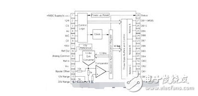
The basic characteristics and parameters of the AD574 are as follows: the AD574 has a 12-bit successive comparison analog-to-digital converter with internal sample and hold; the conversion rate is 25μs, the bus access time is up to 150ns; the nonlinear error is less than ±1/2LBS or ±1LBS; The data can be output in parallel with 12-bit or 8-bit C mode; the four unipolar or bipolar voltage input ranges are ±5V, ±IOV, 0V~10V and 0V~20V respectively; using dual power supply mode, the analog circuit voltage is ± l2V or ±l5V, digital circuit voltage is ±5V.
1.2AD574 pin function and timing control
The following logic is required for the logic control of the AD574: data output bit select input 12/8, chip select signal input CS, read/convert status input R/C, operation enable terminal CE, bit addressing / short cycle conversion The input terminal AO and the conversion state output terminal STS are selected.
When CE=1 and CS=0 are satisfied, the AD574 starts to work normally. When the AD574 is in operation, R/C=0, AID conversion is started; when R/C=1, data is read. The data output bit selects the input 12/8 and AO terminals to control the mode in which the conversion is initiated and the data output format. When AO=0, the startup conversion mode is performed in the complete 12-bit AID conversion mode; when AO=1, the 8-bit A/D conversion mode is performed. When R/C=1, AD574 is in the data state, at this time AO and data output bit selection input 12/8 control the format of data output. When 12/8=1, the data is output in parallel with 12 bits; when 12/8=0, the data is output twice in 8 bits; and when AO=0, the upper 8 bits of the A/D conversion data are output; When AO=1, the lower 4 bits of the A/D conversion data are output, and the lower four bits of the converted data occupy the upper nibble of one byte, and the lower nibble is padded with zero.
The working timing of the AD574 is shown in the figure below.
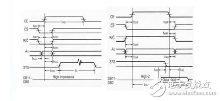
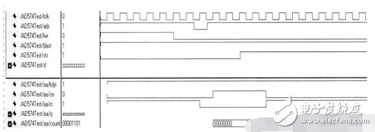
In the system design, the AD574 is connected to the PCI interface chip PCI9052 for data transmission. The conversion control and read data control signals of the AD574 are taken from the pins of the PCI9052. The converted data is transmitted to the MCU through the PCI bus for analysis and processing under the control of the PCI9052. The logic control and timing control of PCI9052 to AD574 are realized by CPLD design. The corresponding timing is shown in Figure 4.
In the timing diagram, ADS#, BLAST, LRDYi, and LCLK are the signal pins of the PCI bus interface chip PCI9052. ADS# is the address latch pin that initiates an access on the PCI bus to control the sampling time of the AD574; BLAST is the last data period of the last access on the PCI bus to control the data reading of the AD574; LRDYi is the slave When the pin is prepared, the PCI9052 can start to read and write data to the local device. The valid signal for controlling the data conversion of the AD574 is started to start reading data. LCLK is a local clock signal generated by the PCI9052. Control timing logic.
2CPLD design and implementation Based on VerilogHDL hardware description language, the ADC574 sampling control design source program is as follows:
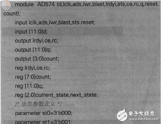
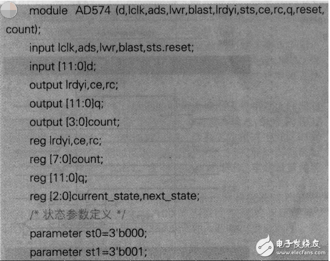
The signal definition in the code corresponds to the pin in the timing diagram of Figure 2. At the same time, a counter is designed to control the timing of the AD574 to meet the conversion accuracy and read requirements of the AD574.
QUARTus 11 software provides a complete, powerful design environment for programmable system-on-chip (SOPC) design. After selecting the CPLD device series according to the needs, the Vielog HDL language input method is used to write the control combination logic code and the test excitation code, and the Quartus 11 software leucorrhea tool is used to analyze the integrated code for routing, layout, resource allocation, and analysis timing and waveform simulation. . Quartus11 also provides a friendly interface to third-party EDA tool software, which can be simulated directly by calling Modelsim software in Quartus 11.
The Quartus 11 6.0 and Modelsim6.1 software systems use approximately 50% of the resources on the MAX3000A Series of programmable devices to control the sampling, AID conversion, and data read of the AD574. The results of the simulation in Mod-elsim6.1 software are shown in the figure below.
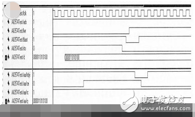
After verification, the circuit can smoothly and conveniently control the operation and operation of the AD574. The conversion process and results are in line with the timing logic and accuracy requirements of the AD574.
3. ConclusionThe use of CPLD technology to achieve logic and timing control, simplifying the complexity of the design on the hardware circuit, based on the programmable features of the CPLD, the design circuit can be modified, upgraded and maintained without changing the overall structure of the hardware circuit; The software program reduces the operation instructions, which improves the speed of data processing and reading to some extent.
1.Shape:Conical ,Multi-pyramidal,Columniform,polygonal or conical
2.Material:steel plate.stainless steel compound plate,stainless steel plate,ect.(anticorrosion treatment with hot galvanization,also color polyester power could be coated on the surface)
High strength low alloy steel Q235,Q345,GR65,GR50 to ensure the mechanical properity of microelement in order to ensure the quality of galvanization (other materials are also avaliable on request)
3.Jointing of pole with insert mode,innerflange mode,face to face joint mode
4.Design of pole :against earthquake of 8 grade ,aganist wind pressure of 160
5.Minimum yield strength:355 mpa
6.Minimum ultimate tensile strength :490 mpa
7.Max ultimate tensilestrength:620 mpa
8.Certificate:ISO9001-2000
9.Length:Within 14m once forming without slip joint
10.Welding:It has past flaw testing.Internal and external double welding makes the welding beautiful in shape
11:Packages:Our poles as normal cover by Mat or straw bale at the top and bottom ,anyway also can following by client required , each 40HC or OT can loading how many pcs will calculation base on the client actually specification and data
Our lighting equipment are made from quality sheet from bending,forming,automatic welding and hot galvanization.We can reach one-run machining length of 14m,and can bend sheet thickness up to 25mm.We adopt advanced welding procedures ,automatically weld main joints and reach rank-II welding quality.

Galvanized Steel Pole,Galvanized Steel Electric Pole,Monopole Galvanized Steel Electric Pole,Galvanized Steel Street Lighting Poles
YIXING FUTAO METAL STRUCTURAL UNIT CO.,LTD( YIXING HONGSHENGYUAN ELECTRIC POWER FACILITIES CO.,LTD.) , https://www.chinasteelpole.com