

Recently, some customers have reported that he encountered the following problems when using the STM32F103 C 8T6:
I2C1 uses PB6 and PB7 ports, and timer TIM3 uses PB0\PB1\PB4\PB5 for 4-way PWM. However, in the process of using, there is no problem if only the timer is initialized, but once I2C1 is initialized, the channel 2 ( PB5 ) of the timer cannot generate the PWM wave, but remains high.
The customer consults the manual to know that the default multiplexing function of PB5 is the SMBA pin of I2C1, but its I2C1 is initialized to I2C mode, not initialized to SMBAS mode, and the same method is available for testing on F0. It was originally developed using the standard library, and then tried to use STM32CubeMx for hardware configuration, using the HAL library to create a new project, or the same problem.
As for the above problem, I checked some of the code for the pwm initialization of I2C1 and TIM3d, and found nowhere wrong. First of all, I suspect that the configuration of I2C1 is wrong. I am worried that the customer will be configured to SMBAS mode when I2C1 is configured. With the help of the library code, the next trace of the register configuration was further traced, and no related problems were found in the related register operations.
Here, several pins of the PWM output of TIM3 involve remapping [REMAP]. From the point of view of the pin assignment of the data sheet, if the SMBA mode of I2C1 is not turned on, there should be no conflict.

Here again, the STM32CubeMx is used for the same configuration based on the STM32F103C8, and the results are the same as those reported by the customer. When not turned I2C1, all pins TIM3 normal function; after turning I2C1, TIM3 portions pin PB5 dysfunction. Feel the problem may be in the place of remap with TIM3. Open the important book based on the STM32F1 series---Reference Manual RM0008 , check the place where the TIM3 pin multiplexing REMAP function is introduced.
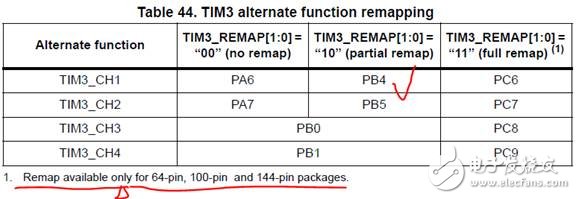
Now the client is performing part of the re-mapping function of TIM3 [partial remap]. From the above table, the current code configuration is no problem. After all, if I don't open I2C1, TIM3 is not abnormal. So come over and check out this place. I don't expect to find obvious errors from here. I am looking forward to finding some additional tips or reminders from nearby. This is not the case. The lower part of the form uses a small one to clearly indicate that the above REMAP operation is only applicable to the 64-pin, 100-pin and 144-pin packages. The chip used by the customer is STM32F103C8, the number of pins is 48, in other words, it It is not supported by the REMAP operation of the multiplexing function of TIM3. At this point, the problem should be said to find the reason.
After a few days, the customer sent an email to continue consulting on the issue. He asked, since the 48-pin chip STM32F1 does not support the REMAP operation of TIM3, why does the PWM function of the 4 pins of TIM3 be normal if I do not turn on I2C1 after REMAP operation; or even if I2C1 is turned on at the same time, PB4 The function is still normal REMAP comes, but the PB5 function is abnormal. I hope I will give further explanation here.
It is normal to have a similar question from the perspective of the user. In fact, since the manual clearly states that the 48-pin STM32F1 chip does not support the REMAP of the TIM3 function pin, it has its own reasons and reasons. If you violate the requirements of the manual, the correctness of the results cannot be guaranteed. Sometimes REMAP is fine, it doesn't mean that there is no problem with REMAP at any time. Just like discussing a certain proposition , local and individual situations are established, and it cannot be said that it is always true . For example, A is 10 years old and B is 20 years old. That is, B is 10 years older than A, and B is twice as old as A this year. Obviously, the two conclusions are established this year. By next year, the latter two times will not be established.
In the application process of the ST MCU, operations similar to those in violation of the manual and the resulting problems often occur. For example, it has been found that when using the flash inside the STM32 chip, it seems that space outside the manual can be used. If the user uses this, the function or characteristics of the chip cannot be guaranteed, and the manufacturer can only guarantee the quality of the area specified in the chip manual. For example, we know that most of the ST MCU chips have UIDs, but some people even send out chips that even if the manual does not have UIDs. They seem to find that such chips still have UIDs and even use them. Ask how this is going on or say Is it reliable? Similarly, for similar situations, the manufacturer can only guarantee the characteristics specified in the manual. Applications that are outside the scope of the manual are the responsibility of the user.
Ok, go back to the topic above.
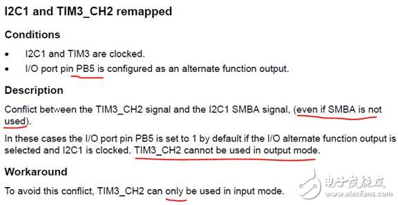
We should find a clear rule or answer from the reference manual for chip applications. We can also check out the more detailed errata based on the chip. Later, the corresponding errata manual was found on the official website. [ Note: The errata manual is often based on the chip model, that is, a series may have multiple errata manuals. ] We also see a detailed description of the above problem in the errata manual, which should be considered Further supplements to the reference manual.
At this point, the cause of the problem is basically clear. Some people may ask, the above mentioned the use of STM32CubeMx for engineering configuration, the configuration process did not find an exception, or the configuration process did not encounter the above obstacles. Since the reference manual does not allow the TIM3 remap operation of the STM32F103C8 chip, when the i2c1 is enabled, the illegal prompt should be displayed when configuring the REMAP function of the TIM3 through the cubeMx.
The version of CUBEMX I am using is 4.22.0. When I2C1 is turned on, and according to the partial REMAP configuration of TIM3, I can't say that no reminder is given. It can only be said that the reminder is not clear enough. The reminder may be easily overlooked and then configured along the way.
The STM32CubeMx is configured as shown below. There is a yellow warning in the place of I2C1. When the mouse is over, there is a text prompt [not necessarily everyone will notice]:
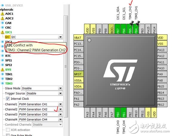
It can be said that CubeMx is still not rigorous or not well thought out. If I2C1 is turned on, it is good to reject the remap of TIM3 when the user tries to configure PB5 as the output . However, this may affect another group of users. They don't care about PB5 at all. Just pay attention to PB4 as a PWM output. A bit of a taste that is difficult to adjust. The reference manual does not support the REMAP operation of the TIM3 of the STM32F1 series 48-pin. It is also supplemented with the errata manual to meet the needs of different applications.
After all, the STM32CubeMX project is vast, and there must be some areas that need improvement, especially similar details. However, we believe that it will be more and more perfect. Anyway, we can't completely leave the chip manual aside at any time. For example , we know that ST official has a firmware library based on each STM32 series. The various sample projects in Curry are very convenient for everyone to learn and develop. It is not difficult to imagine that these firmware library projects are also relatively large, and it is inevitable that there will be bugs, which have been constantly improving. If you encounter any doubts in the process of using them, you may wish to check the relevant data sheet or development reference manual for further comparison confirmation. If you feel that the manual is still not clear enough, you can go to the errata manual of the corresponding chip to see if there is any further explanation of the related issues.
A bunch of smashing, throwing bricks to attract jade.
The GPU slot spacing of this product is 65MM, and the thickness of your graphics card should not exceed 60MM to ensure the normal heat dissipation of the graphics card.
Eth mining rig, including: Motherboard, Intel CPU (with CPU cooler), 4G RAM, case fan, 6 PIN cable to (6 + 2) Pin * 8pcs, , screws Package, win10 system. installation instructionsGPU Port Gap: the port gap between GPUs is 65mm, you can put 8pcs GPUs on the motherboard at the same time if your GPU thickness is less than 60mm, otherwise you will just put only less than 4pcs GPUs on the motherboard at the same time.
Low comsuption: the gpu mining rigs system comsuption is less than 150watt. Good cooling: 3pcs 120mm fan to make sure very good cooling, Case Size: 25.6*15.7*5 Inch, Cooler Fan: 120mm, 5500rpm
Applicable graphics card: NVIDIA: 2070/2080/2060S/2070S/2080S/1080TI/3070/3060TI/3080/3090 AMD: 5600XT/5700/5700XT/6800/6800XT/6900/6900XT/VEGA56/ etc.Noise: 70 decibels
No-load power: 150W
Configuration parameters:CPU: Intel G2950 3.2G
Motherboard: Intel-HM86
Memory: 4GB DDR3
PCIe: GEN3
Software: Windows 10(inactivated)
Built-in interface: 1X MSATA 1 X4G DDR3L 8PCIe X1 GEN3
External interface: 1 VGA (and HDMI adapter cable) 1GB network interface USB 2 2.0
Power interface: 10X6pin
ETH/ETC/AE/BTM/GRIN/GRIN31/BEAM/SERO/RVN/MONA/CKB/XVG/BCD/FIRO/HYC/VTC/CLO/RVC/PGN/CHI etc.
crypto mining rig,bitcoin mining rig,mining rig for sale,cryptocurrency mining rig,how to build a mining rig
Easy Electronic Technology Co.,Ltd , https://www.yxpcelectronicgroups.com