
Spartan-6 has a wealth of I/O resources, including SelecTIO and RockeTIO.
Each I/O slice (TIle) of Spartan-6 contains two IOBs, two ILOGIC2s, two OLOGIC2s, and two IODELAY2s, as shown in Figure 2-37.
In this section, the Spartan-6 SelectIO resources are introduced in the following sections.
The electrical characteristics of SelectIO.
SelectIO's logic resources (ILOGIC2, OLOGIC2).
SelectIO's advanced logic resources (ISERDES, OSERDES, Bitslip).
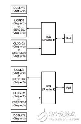
Figure 2-37 I / O slice structure
First, the electrical characteristics of SelectIO IOBAll Spartan-6 FPGAs feature high performance configurable SelectIO drivers and receivers that support a wide range of interface standards. The output strength, slope, and on-chip termination OCT of the I/O can be programmed.
Each IOB contains input, output, and tri-state SelectIO drivers. These drives can be configured to a variety of I/O standards.
Single-ended I/O standards (LVCMOS, LVTTL, HSTL, SSTL, PCI).
Differential I/O standards (LVDS, RSDS, TMDS, differential HSTL, and SSTL).
Note: The differential input and VREF related inputs are powered by VCCAUX.
The Xilinx software library provides many primitives for Spartan-6 I/O, including IBUF (input buffer) for single-ended signals, IBUFG (clock input buffer), OBUF (output buffer), and OBUFT (three-state output). Buffer) and IOBUF (input/output buffer); and IBUFDS (input buffer) for differential signals, IBUFGDS (clock input buffer), OBUFDS (output buffer), OBUFTDS (three-state output buffer), and IOBUFDS (input/output buffer).
Second, the logical resources of SelectIOThe logical resources of SelectIO refer to the logic behind the I/O driver and receiver, and contain all the basic I/O logic resources of the Spartan-6 FPGA, as shown in Figure 2-38. The resources included are as follows.
Combine input/output.
Three-state output control.
Register input/output.
Register three-state output control.
Double data rate (DDR) input/output.
DDR output tri-state control.
IODELAY2 provides control of high resolution adjustable delay units.
Supports DDR output of three alignment modes of NONE, C0 and C1.
Supports DDR inputs in three alignment modes: NONE, C0, and C1.
ISERDES.
OSERDES.
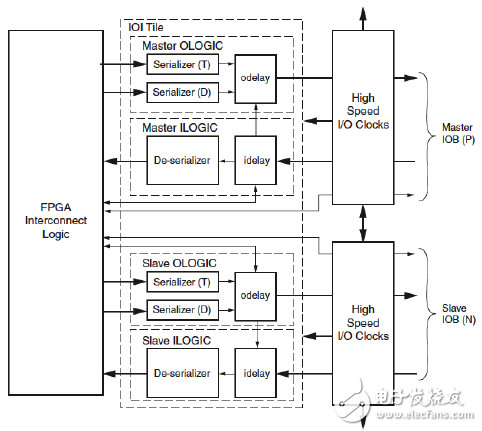
Figure 2-38 SelectIO logical resources in I/O slices
An I/O slice (IOI) manages two IOBs. The IOI consists of two single-ended inputs/outputs, or a complete circuit for differential input/output and an internal interconnect module. The two IOBs are combined to support a high speed differential interface.
In single-ended mode, the main IOB drives pin P and the IOB drives pin N. In differential mode, the master-slave IOBs can be combined to achieve serial-to-parallel conversion, and the data rate is 1 to 2 times that of single-ended mode. Each I/O supports three configuration modes: latched I/O, non-locked I/O, and Registered I/O. I/O can also be configured as a 2:1/3:1/4:1 SERDES. The latch/register clock is derived from the GCLK-driven global clock network or the high-speed I/O clock network.
IODELAY2 is an optional resource. The designer can add this delay module to the input/output path as needed. The delay of IODELAY2 is programmable and can be specified by DRP or by instantiating the IODELAY2 primitive. This delay can be either a fixed delay or a variable delay.
Third, ILOGIC2 resourcesFigure 2-39 shows the ILOGIC2 logic block diagram, which supports the following features.
The edge triggers the D-type flip-flop.
IDDR (NONE, C0 or C1) mode.
Latches.
Asynchronous/combination logic.
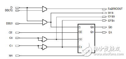
Figure 2-39 ILOGIC2 logic block diagram
(1) Asynchronous/combination logic.
When one of the following conditions occurs, the software automatically generates a combined path that allows the input driver to be directly connected to the internal logic resources of the FPGA.
The input data of the FPGA is directly connected to the internal logic, and no registers are used.
The attribute "Package I/O Register/Latch to IOB" is set to OFF.
(2) IDDR mode.
ILOGIC2 in Spartan-6 devices has dedicated registers to implement the Input Double Data Rate (DDR) registers. This feature can be used by instantiating the primitives of IDDR2.
IDDR2's attribute DDR_ALIGNMENT has three modes: NONE, C0, and C1.
In NONE mode, the input DDR timing is shown in Figure 2-40. The register registers input data D to Q0 on the rising edge of C0, and the next input data D is registered to Q1 on the rising edge of C1.
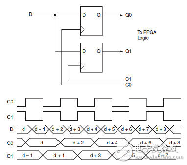
Figure 2-40 Schematic diagram of input DDR timing when DDR_ALIGNMENT=NONE
In some cases, the input data must be synchronized to a clock domain, usually C0 is synchronized. However, in the case of higher frequencies, this synchronization is relatively difficult because the effective time is only half of the clock period (in the case of 50% duty cycle). IDDR2 in Spartan-6 devices contains dedicated logic for clock domain synchronization within ILOGIC2.
When DDR_ALIGNMENT is C0 (or C1), signal Q0 (Q1) is registered again at C1 (C0), and the input data is synchronized to the same clock domain through the internal interconnect. The timing diagram is shown in Figure 2-41.
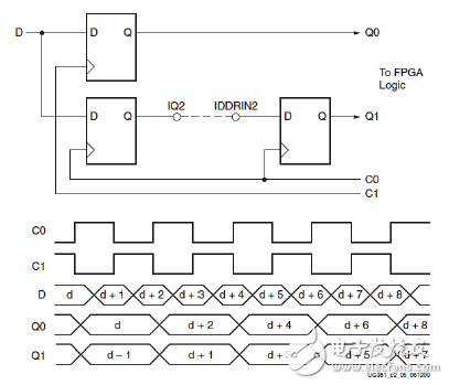
Figure 2-41 Input DDR of DDR_ALIGNMENT=C0\C1
The primitives of IDDR are shown in Figure 2-42.
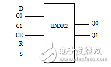
Figure 2-42 Primitives of IDDR2
Fourth, OLOGIC2 resourcesAs shown in Figure 2-43, OLOGIC2 consists of two parts: the output data path and the three-state control path.
These two parts can be configured in the following modes.
The edge triggers a D-type flip-flop.
DDR mode (NONE, C0 or C1 sync mode).
Level sensitive latch.
Asynchronous/combination logic.
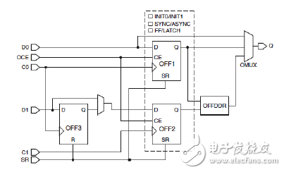
Figure 2-43 OLOGIC2 logic module
(1) Combined data output and tri-state control path.
When one of the following conditions occurs, the software automatically generates a combined path to output the FPGA internal data directly to the output of the output driver or driver.
The FPGA internal logic data is directly output to the output driver or the three-state control terminal of the driver without passing through the registers.
The attribute "Packet I/O Register/Latch to IOB" is set to OFF.
(2) ODDR mode.
297W Charging Medical Power Supply
297W Charging Medical Power Supply,297W Medical Device Power Supply,297W Medical Power Adapter,297W Rade Power Supplies
Shenzhen Longxc Power Supply Co., Ltd , https://www.longxcpower.com