
Abstract: Class D amplifiers generally have higher efficiency than class AB amplifiers and are suitable for low-power applications. However, despite the inherent advantages of Class D amplifiers, they still cannot compensate for the shortcomings of traditional Class D amplifiers, that is, they increase costs, reduce audio performance, and require output filtering. However, in recent years, advances in Class D amplifier technology have reduced the cost of Class D amplifiers, while providing similar audio performance as Class AB amplifiers. In addition, some new class D output modulation schemes also reduce EMI in many applications.
Introduction The technology of Class D amplifiers has developed rapidly in recent years, and the most common is that it is used in low-power products with less than 50W per channel. In these low-power applications, Class D amplifiers have inherent advantages in efficiency compared to traditional Class AB amplifiers, because the output stage of Class D amplifiers is usually only on or off, and there is no intermediate bias stage. However, for a long time, this efficiency advantage did not make it widely favored by designers, because Class D amplifiers also have obvious disadvantages: high device cost, poor audio performance (compared to Class AB amplifiers), and Output filtering is required.
In recent years, affected by the following two main factors, this situation is gradually reversed, making Class D amplifiers arouse people's extensive attention in many application fields.
First, it is the market. Certain advantages of Class D amplifiers have driven the rapid development of the two terminal device markets, mobile phones and LCD flat panel displays. For mobile phones, the speaker and PTT (Push-to-Talk) mode requires the high efficiency of Class D amplifiers to extend battery life. The development of LCD flat panel displays puts forward a demand for "cool running" for electronic devices, because the increase in operating temperature will affect the display color contrast. The high efficiency of Class D amplifiers means that the power consumption when driving electronic devices is lower, so that the LCD flat panel display works less heat, and the image display effect is better.
The second factor affecting the application of Class D amplifiers is the development of its own technology. According to market needs, some manufacturers have improved Class D amplification technology to make Class D amplifiers have a more ideal price, but also have audio performance similar to Class AB amplifiers. In addition, some new class D amplifier output modulation schemes can also reduce EMI in practical applications.
Although some new class D amplification design schemes are based on the old-style PWM structure, they use more complex modulation techniques to achieve filter-free operation in low-power systems. The efficiency index can be verified by testing, but some designers still suspect that products based on these new technologies will have general EMC / RFI compatibility issues. In fact, a good PCB layout and shorter speaker wiring can ensure that EMI radiation is greatly reduced to meet FCC or CE standards. Difficulties in application The physical layout in some applications requires long speaker wiring. Such speaker wiring has an antenna effect, and RF radiation must be strictly controlled. In fact, the longer the speaker cable is, the lower the frequency it generates radiation as an antenna. At the same time, some applications require EMI radiation to be lower than the CE / FCC standard to comply with automotive electronics specifications or to avoid interference with other low-frequency circuits. Faced with such diverse demands, these applications often become difficult to overcome.
The most representative application difficulty is the flat-screen TV. Since the speakers are usually arranged on the outer edge of the device, it is often inevitable to use long speaker cables. If there are still analog video signals, it is not enough to meet the RF radiation requirements of FCC or CE (these standards are only for frequencies above 30MHz); often the switching fundamental frequency needs to be suppressed to avoid interference with the video signal. If the traditional LC filters used in early PWM amplifiers are used, they need to be analyzed to ensure that they can effectively suppress the high-frequency switching transients generated by the new amplifiers. PWM Type D Amplifier Traditional Class D amplifiers are usually designed based on the principle of pulse width modulation (PWM). Its output can be configured as a single-ended or fully differential bridged load (BTL). Figure 1 shows the typical BTL output waveform of a PWM type D amplifier. The fast switching time and the rail-to-rail swing make this type of amplifier very efficient. However, these characteristics make the amplifier have a wide output spectrum, which may cause high-frequency RF radiation and interference. Therefore, the use of such schemes usually requires the use of output filters to suppress harmful RF radiation.
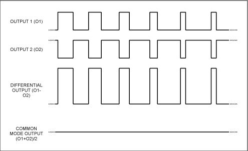
Figure 1. Waveform of traditional pulse width modulation (PWM) scheme
As shown in Figure 1, if the device's inverting and non-inverting output loops have a high degree of matching, the two symmetrical output signal waveforms will have a small common-mode (CM) signal on the speaker or wiring (the bottom trace line). Note: 50% duty cycle represents zero input signal (idle state). Therefore, a differential low-pass filter can be designed to attenuate high-frequency components (produced by rapid switching) in the signal waveform, while retaining useful low-frequency components for output to the speaker. New Generation Modulation Technology With the growing demand for Class D amplifiers in the market, some manufacturers have recently introduced new generation modulation schemes that can independently control the two half-bridges of the H-bridge. This modulation scheme has two main advantages: When the audio signal is weak or idle, there is almost no differential switching signal on the load. Compared with the traditional PWM design, the quiescent current consumption is improved. The minimum pulse, common mode (CM) switching signal helps reduce turn-on and turn-off transients. The idle DC level (after filtering) of the BTL output pin is close to GND. Therefore, filter element mismatch or stray capacitance (which may cause audio noise when the amplifier is turned on or off) can be minimized. Obviously, although this new technology has some advantages, the amplifier output will no longer be symmetrical. The signal waveform shown in Figure 2 (using the MAX9704 stereo Class D amplifier as an example) has a high common-mode component.
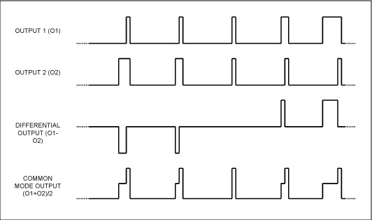
Figure 2. Maxim's MAX9704 stereo Class D amplifier modulation scheme
The output filter requirements of this class D amplifier are different from those with traditional differential inputs and complementary PWM outputs. Compared with PWM, the output of the MAX9704 modulation scheme often contains a higher common-mode signal, which needs to be considered when designing the output filter. As the following examples show, the effect of traditional differential filter topologies is often less than ideal.
Figure 3a shows the traditional PWM type D output LC filter and its ideal value. For simplicity, it can be assumed that the speaker load has an ideal 8Ω resistance, and the DC resistance of the inductor is ignored. Through some simple SPICE simulations, the problem can be obtained. Figure 3b shows the frequency response of the filter in Figure 3a to the differential input signal. The response curves of two output nodes (FILT1, FILT2) relative to GND are given. The device values ​​shown in the figure have an ideal second-order roll-off above 30kHz and ideal transients. The group delay characteristic in the audio band remains flat within 4µs.
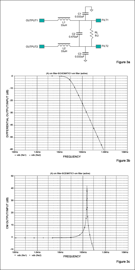
Figure 3. (a) Traditional differential mode passive LC filter, (b) frequency response for differential input signals, (c) frequency response for common mode signals.
Figure 3c shows the output of the same filter with a common-mode input. Similarly, the response curves of both outputs are relative to GND. The output result (Y-axis offset) has a large peak and obvious underdamping. Combined with the equivalent circuit of the filter under the common mode signal (Figure 4), it is easy to understand why this result occurs. Because the ideally matched inductors and capacitors are used in the simulation, the differential signal on the resistive load is zero, so there will be no attenuation of the LC components. L1 and C1 resonate (L2 and C3 are the same) and produce a peak. In the time domain (not shown in the figure), this situation will have large overshoot and oscillation. Note that when a common-mode signal is input, C2 will introduce a zero. Therefore, the cut-off frequency of the filter (referred to as the resonance frequency at this time may be more accurate) will be higher than the cut-off frequency of the differential input.
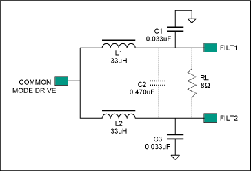
Figure 4. Under the common mode input, the equivalent circuit of the traditional LC filter in Figure 3a.
At this time, you may ask, is there any problem? If the common-mode energy of the output spectrum at this frequency is zero, then there is no problem. However, if the peak frequency is exactly equal to the switching frequency of the Class D amplifier, a larger output voltage amplitude will appear on the speaker and the wiring. At the same time, the spread spectrum modulation (SSM) mode of the MAX9704 will cause the underdamped filter to introduce considerable noise above the audio band. Spread spectrum mode is pin-selectable. At this time, the high-frequency switching energy is "white noise", and the noise amplitude can be reduced by randomly adjusting the switching time cycle by cycle. This spread spectrum scheme simplifies the design of EMI compatibility in filterless applications. Underdamped Common Mode Response Problem One of the solutions to the above common mode problem is to retain the basic structure of Figure 3a, but add a damping element that suppresses high resonance common mode signals. Figure 5a shows a series RC element between the two output nodes and GND. If the efficiency requirements in the application are not very high, only one resistor can be connected between the output node and GND, but capacitors C4 and C5 will help reduce the additional power loss on R1 and R2.
The values ​​of C4 and C5 should be weighed and selected: on the one hand, increasing the values ​​of C4 and C5 helps R1 and R2 to attenuate the peak, on the other hand, C4 and C5 should be reduced to reduce the loss of high-frequency audio (up to 20kHz). If the common-mode cut-off frequency is much greater than the differential-mode frequency, it is easy to choose, for example, only by increasing the ratio of C2 to C1 and C3 can be achieved. Increasing the common-mode cutoff frequency can reduce the values ​​of C4 and C5, while increasing the values ​​of R1 and R2, which will reduce the audio loss on R1 and R2. If the common-mode cut-off frequency is too high, the common-mode components on the cable will be too much. Therefore, the ratio of the -3dB frequency point of the differential and common mode must be properly selected. The filter in this case uses a ratio of 1: 5.
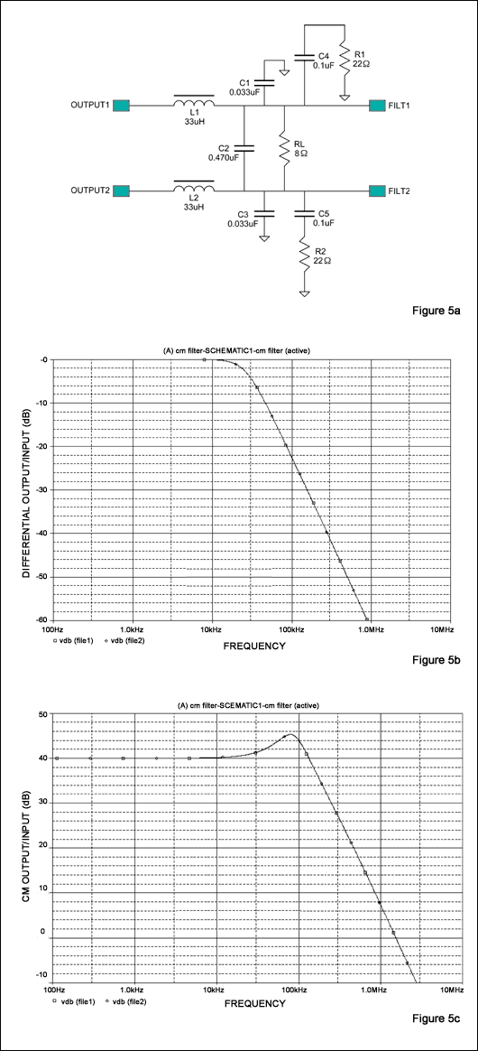
Figure 5. Adding an RC network (a) to each output of a traditional LC filter can improve the frequency response of differential signals (b) and the frequency response of common-mode signals (c).
Figure 5b is the response of the filter of Figure 5a to the differential input, and Figure 5c is the response of the common-mode input. Note: The common-mode cut-off frequency in Figure 5c is higher (-3dB bandwidth is about 110kHz, differential input is 28kHz), with smooth and reasonably controlled spikes. The cutoff frequency is much higher than the highest audio frequency (also lower than the fundamental frequency of the class D switching frequency), so it has a good effect.
Some low switching frequency (200kHz to 300kHz) applications are not suitable for the scheme shown in Figure 5c. For such products may need to use other methods and topologies. The MAX9704 stereo class-D amplifier (Figure 6) can be set to 940kHz fixed-frequency mode (FFM) (FS1 = low, FS2 = high), at which point the effect is best. The MAX9704 operating in FFM mode sets the switching period to a constant value (with three options) through pin selection to meet application requirements.
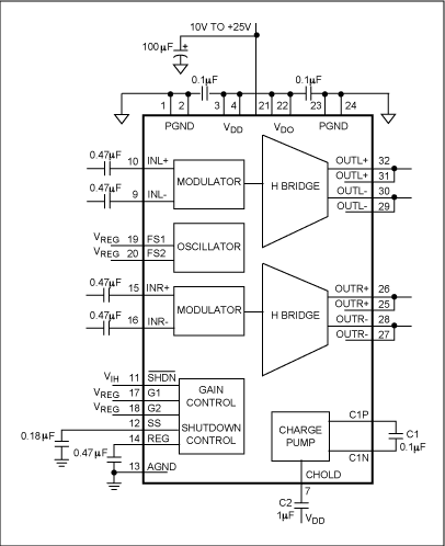
Figure 6. Typical application circuit of the MAX9704 stereo Class D power amplifier
Figures 7 and 8 show the time-domain performance when using the filter of Figure 5 to filter the MAX9704. The load impedance is 8Ω in both cases. Figure 7 also shows the waveforms of the FILT1 and FILT2 nodes (top trace) and the resulting 1kHz differential output waveform (bottom trace). The noise of the top trace is the residual signal after the output switching signal is filtered (the power supply voltage is 15V). Figure 8 is a detailed display of the trace of Figure 7. Note: The ripple mainly comes from the 940kHz switching frequency, and the two channels appear in the form of common mode signals. It should also be noted that there are no higher harmonics on the output, indicating that EMI has been effectively suppressed (the initial test frequency of radiated EMI is usually higher than 30MHz).
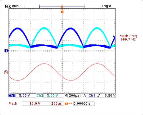
Figure 7. The signal waveforms generated on FILT1 and FILT2 when the MAX9704 is used to drive the circuit in Figure 5a (simultaneously shown on the top trace), and the differential output (bottom trace).
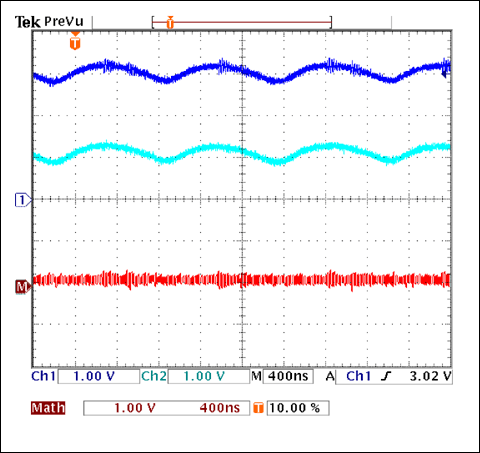
Figure 8. The top trace shows the residual ripple voltage in the output of the circuit in Figure 5a. The ripple component is mainly the fundamental frequency of the switching frequency (940kHz at this time). The second-order roll-off of the filter above this frequency point suppresses all higher harmonics well. Ripple has almost only common-mode components (bottom trace). Relevant notes The filter designs discussed in this article assume a load impedance of 8Ω. The voice coil inductance causes the impedance of most wide range dynamic coil speakers to become higher in the frequency range of 20 kHz. This feature helps to achieve high-efficiency filter-less operation, but when selecting filtering devices to reduce EMI, the rise in impedance should be considered.
When trying to evaluate and describe the characteristics of Class D amplifiers, in order to select and evaluate devices, audio designers often need to filter even in a laboratory environment. Even if the final product without the filter can pass the EMC test, the problem can still be found through the amplifier performance test. Many audio analyzers are specifically designed to measure the THD + N or amplitude response of traditional audio amplifiers. When used to test filterless Class D amplifiers, errors often occur. The circuit shown in Figure 5 is suitable for testing (correctly loading an 8Ω resistive load), but it should be noted that the nonlinearity that may be introduced by the 33µH inductance will limit the THD measurement. Air gap components often have the best measurement results, but the size often limits their application in actual products!
In recent years, affected by the following two main factors, this situation is gradually reversed, making Class D amplifiers arouse people's extensive attention in many application fields.
First, it is the market. Certain advantages of Class D amplifiers have driven the rapid development of the two terminal device markets, mobile phones and LCD flat panel displays. For mobile phones, the speaker and PTT (Push-to-Talk) mode requires the high efficiency of Class D amplifiers to extend battery life. The development of LCD flat panel displays puts forward a demand for "cool running" for electronic devices, because the increase in operating temperature will affect the display color contrast. The high efficiency of Class D amplifiers means that the power consumption when driving electronic devices is lower, so that the LCD flat panel display works less heat, and the image display effect is better.
The second factor affecting the application of Class D amplifiers is the development of its own technology. According to market needs, some manufacturers have improved Class D amplification technology to make Class D amplifiers have a more ideal price, but also have audio performance similar to Class AB amplifiers. In addition, some new class D amplifier output modulation schemes can also reduce EMI in practical applications.
Although some new class D amplification design schemes are based on the old-style PWM structure, they use more complex modulation techniques to achieve filter-free operation in low-power systems. The efficiency index can be verified by testing, but some designers still suspect that products based on these new technologies will have general EMC / RFI compatibility issues. In fact, a good PCB layout and shorter speaker wiring can ensure that EMI radiation is greatly reduced to meet FCC or CE standards. Difficulties in application The physical layout in some applications requires long speaker wiring. Such speaker wiring has an antenna effect, and RF radiation must be strictly controlled. In fact, the longer the speaker cable is, the lower the frequency it generates radiation as an antenna. At the same time, some applications require EMI radiation to be lower than the CE / FCC standard to comply with automotive electronics specifications or to avoid interference with other low-frequency circuits. Faced with such diverse demands, these applications often become difficult to overcome.
The most representative application difficulty is the flat-screen TV. Since the speakers are usually arranged on the outer edge of the device, it is often inevitable to use long speaker cables. If there are still analog video signals, it is not enough to meet the RF radiation requirements of FCC or CE (these standards are only for frequencies above 30MHz); often the switching fundamental frequency needs to be suppressed to avoid interference with the video signal. If the traditional LC filters used in early PWM amplifiers are used, they need to be analyzed to ensure that they can effectively suppress the high-frequency switching transients generated by the new amplifiers. PWM Type D Amplifier Traditional Class D amplifiers are usually designed based on the principle of pulse width modulation (PWM). Its output can be configured as a single-ended or fully differential bridged load (BTL). Figure 1 shows the typical BTL output waveform of a PWM type D amplifier. The fast switching time and the rail-to-rail swing make this type of amplifier very efficient. However, these characteristics make the amplifier have a wide output spectrum, which may cause high-frequency RF radiation and interference. Therefore, the use of such schemes usually requires the use of output filters to suppress harmful RF radiation.
Figure 1. Waveform of traditional pulse width modulation (PWM) scheme
As shown in Figure 1, if the device's inverting and non-inverting output loops have a high degree of matching, the two symmetrical output signal waveforms will have a small common-mode (CM) signal on the speaker or wiring (the bottom trace line). Note: 50% duty cycle represents zero input signal (idle state). Therefore, a differential low-pass filter can be designed to attenuate high-frequency components (produced by rapid switching) in the signal waveform, while retaining useful low-frequency components for output to the speaker. New Generation Modulation Technology With the growing demand for Class D amplifiers in the market, some manufacturers have recently introduced new generation modulation schemes that can independently control the two half-bridges of the H-bridge. This modulation scheme has two main advantages: When the audio signal is weak or idle, there is almost no differential switching signal on the load. Compared with the traditional PWM design, the quiescent current consumption is improved. The minimum pulse, common mode (CM) switching signal helps reduce turn-on and turn-off transients. The idle DC level (after filtering) of the BTL output pin is close to GND. Therefore, filter element mismatch or stray capacitance (which may cause audio noise when the amplifier is turned on or off) can be minimized. Obviously, although this new technology has some advantages, the amplifier output will no longer be symmetrical. The signal waveform shown in Figure 2 (using the MAX9704 stereo Class D amplifier as an example) has a high common-mode component.
Figure 2. Maxim's MAX9704 stereo Class D amplifier modulation scheme
The output filter requirements of this class D amplifier are different from those with traditional differential inputs and complementary PWM outputs. Compared with PWM, the output of the MAX9704 modulation scheme often contains a higher common-mode signal, which needs to be considered when designing the output filter. As the following examples show, the effect of traditional differential filter topologies is often less than ideal.
Figure 3a shows the traditional PWM type D output LC filter and its ideal value. For simplicity, it can be assumed that the speaker load has an ideal 8Ω resistance, and the DC resistance of the inductor is ignored. Through some simple SPICE simulations, the problem can be obtained. Figure 3b shows the frequency response of the filter in Figure 3a to the differential input signal. The response curves of two output nodes (FILT1, FILT2) relative to GND are given. The device values ​​shown in the figure have an ideal second-order roll-off above 30kHz and ideal transients. The group delay characteristic in the audio band remains flat within 4µs.
Figure 3. (a) Traditional differential mode passive LC filter, (b) frequency response for differential input signals, (c) frequency response for common mode signals.
Figure 3c shows the output of the same filter with a common-mode input. Similarly, the response curves of both outputs are relative to GND. The output result (Y-axis offset) has a large peak and obvious underdamping. Combined with the equivalent circuit of the filter under the common mode signal (Figure 4), it is easy to understand why this result occurs. Because the ideally matched inductors and capacitors are used in the simulation, the differential signal on the resistive load is zero, so there will be no attenuation of the LC components. L1 and C1 resonate (L2 and C3 are the same) and produce a peak. In the time domain (not shown in the figure), this situation will have large overshoot and oscillation. Note that when a common-mode signal is input, C2 will introduce a zero. Therefore, the cut-off frequency of the filter (referred to as the resonance frequency at this time may be more accurate) will be higher than the cut-off frequency of the differential input.
Figure 4. Under the common mode input, the equivalent circuit of the traditional LC filter in Figure 3a.
At this time, you may ask, is there any problem? If the common-mode energy of the output spectrum at this frequency is zero, then there is no problem. However, if the peak frequency is exactly equal to the switching frequency of the Class D amplifier, a larger output voltage amplitude will appear on the speaker and the wiring. At the same time, the spread spectrum modulation (SSM) mode of the MAX9704 will cause the underdamped filter to introduce considerable noise above the audio band. Spread spectrum mode is pin-selectable. At this time, the high-frequency switching energy is "white noise", and the noise amplitude can be reduced by randomly adjusting the switching time cycle by cycle. This spread spectrum scheme simplifies the design of EMI compatibility in filterless applications. Underdamped Common Mode Response Problem One of the solutions to the above common mode problem is to retain the basic structure of Figure 3a, but add a damping element that suppresses high resonance common mode signals. Figure 5a shows a series RC element between the two output nodes and GND. If the efficiency requirements in the application are not very high, only one resistor can be connected between the output node and GND, but capacitors C4 and C5 will help reduce the additional power loss on R1 and R2.
The values ​​of C4 and C5 should be weighed and selected: on the one hand, increasing the values ​​of C4 and C5 helps R1 and R2 to attenuate the peak, on the other hand, C4 and C5 should be reduced to reduce the loss of high-frequency audio (up to 20kHz). If the common-mode cut-off frequency is much greater than the differential-mode frequency, it is easy to choose, for example, only by increasing the ratio of C2 to C1 and C3 can be achieved. Increasing the common-mode cutoff frequency can reduce the values ​​of C4 and C5, while increasing the values ​​of R1 and R2, which will reduce the audio loss on R1 and R2. If the common-mode cut-off frequency is too high, the common-mode components on the cable will be too much. Therefore, the ratio of the -3dB frequency point of the differential and common mode must be properly selected. The filter in this case uses a ratio of 1: 5.
Figure 5. Adding an RC network (a) to each output of a traditional LC filter can improve the frequency response of differential signals (b) and the frequency response of common-mode signals (c).
Figure 5b is the response of the filter of Figure 5a to the differential input, and Figure 5c is the response of the common-mode input. Note: The common-mode cut-off frequency in Figure 5c is higher (-3dB bandwidth is about 110kHz, differential input is 28kHz), with smooth and reasonably controlled spikes. The cutoff frequency is much higher than the highest audio frequency (also lower than the fundamental frequency of the class D switching frequency), so it has a good effect.
Some low switching frequency (200kHz to 300kHz) applications are not suitable for the scheme shown in Figure 5c. For such products may need to use other methods and topologies. The MAX9704 stereo class-D amplifier (Figure 6) can be set to 940kHz fixed-frequency mode (FFM) (FS1 = low, FS2 = high), at which point the effect is best. The MAX9704 operating in FFM mode sets the switching period to a constant value (with three options) through pin selection to meet application requirements.
Figure 6. Typical application circuit of the MAX9704 stereo Class D power amplifier
Figures 7 and 8 show the time-domain performance when using the filter of Figure 5 to filter the MAX9704. The load impedance is 8Ω in both cases. Figure 7 also shows the waveforms of the FILT1 and FILT2 nodes (top trace) and the resulting 1kHz differential output waveform (bottom trace). The noise of the top trace is the residual signal after the output switching signal is filtered (the power supply voltage is 15V). Figure 8 is a detailed display of the trace of Figure 7. Note: The ripple mainly comes from the 940kHz switching frequency, and the two channels appear in the form of common mode signals. It should also be noted that there are no higher harmonics on the output, indicating that EMI has been effectively suppressed (the initial test frequency of radiated EMI is usually higher than 30MHz).
Figure 7. The signal waveforms generated on FILT1 and FILT2 when the MAX9704 is used to drive the circuit in Figure 5a (simultaneously shown on the top trace), and the differential output (bottom trace).
Figure 8. The top trace shows the residual ripple voltage in the output of the circuit in Figure 5a. The ripple component is mainly the fundamental frequency of the switching frequency (940kHz at this time). The second-order roll-off of the filter above this frequency point suppresses all higher harmonics well. Ripple has almost only common-mode components (bottom trace). Relevant notes The filter designs discussed in this article assume a load impedance of 8Ω. The voice coil inductance causes the impedance of most wide range dynamic coil speakers to become higher in the frequency range of 20 kHz. This feature helps to achieve high-efficiency filter-less operation, but when selecting filtering devices to reduce EMI, the rise in impedance should be considered.
When trying to evaluate and describe the characteristics of Class D amplifiers, in order to select and evaluate devices, audio designers often need to filter even in a laboratory environment. Even if the final product without the filter can pass the EMC test, the problem can still be found through the amplifier performance test. Many audio analyzers are specifically designed to measure the THD + N or amplitude response of traditional audio amplifiers. When used to test filterless Class D amplifiers, errors often occur. The circuit shown in Figure 5 is suitable for testing (correctly loading an 8Ω resistive load), but it should be noted that the nonlinearity that may be introduced by the 33µH inductance will limit the THD measurement. Air gap components often have the best measurement results, but the size often limits their application in actual products!
Copper Wire Lights,Copper Fairy Lights,Copper Wire Fairy Lights,Wire Fairy Lights
DONGGUAN JIANXING LIGHTING ELECTRIC APPLIANCES CO., LTD , https://www.rslightstring.com