
Abstract: The high-efficiency characteristics of Class D amplifiers make them ideal for portable and high-power applications. Traditional Class D amplifiers require an external low-pass filter to extract audio signals from the output waveform of a pulse-width modulated signal (PWM). However, many modern Class D amplifiers use advanced modulation techniques, which can eliminate external filters and reduce electromagnetic interference (EMI) in various applications. Eliminating the external filter not only reduces the space requirements of the circuit board, but also greatly reduces the cost of many portable / compact applications.
Introduction Most audio system design engineers are well aware that Class D amplifiers have considerable advantages in efficiency compared to linear audio amplifiers (such as Class A, Class B, and Class AB). For linear amplifiers (such as class AB), the linear operation of the biasing element and output transistor consumes a lot of power. Because the transistors of Class D amplifiers are only used as switches to control the direction of the current flowing through the load, the power consumption of the output stage is extremely low. The power consumption of Class D amplifiers mainly comes from the output impedance of the output transistors, switching losses and quiescent current overhead. The power consumption of the amplifier is mainly dissipated in the form of heat. Class D amplifiers have greatly reduced heat sink requirements and can even eliminate heat sinks, making them ideal for compact high-power applications.
In the past, the typical class-D amplifier based on the PWM method required external filtering components, which would cause EMI / EMC compatibility problems, and the THD + N performance was poor. Therefore, its high-efficiency advantage was greatly lost compared with the linear amplifier. However, the latest generation of Class D amplifiers uses advanced modulation and feedback techniques to alleviate the above problems.
Basics of Class D Amplifiers Modern Class D amplifiers use a variety of modulator topologies, and the most basic topology combines pulse-width modulation (PWM) and triangular (or sawtooth) oscillators. Figure 1 shows a simplified block diagram of a PWM-based half-bridge Class D amplifier. It includes a pulse width modulator, two output MOSFETs, and an external low-pass filter (LF and CF) to recover the amplified audio signal. As shown in the figure, p-channel and n-channel MOSFETs are used as current steering switches, and their output nodes are alternately connected to VDD and ground. Because the output transistor switches the output between VDD and ground, the final output of the Class D amplifier is a high-frequency square wave. The switching frequency (fSW) of most Class D amplifiers is usually between 250kHz and 1.5MHz. The audio input signal performs pulse width modulation on the output square wave. The audio input signal is compared with the triangle wave (or sawtooth wave) generated by the internal oscillator to obtain a PWM signal. This modulation method is usually called "natural sampling", in which the triangular wave oscillator is used as the sampling clock. The duty cycle of the square wave is proportional to the input signal level. When there is no input signal, the duty cycle of the output waveform is 50%. Figure 2 shows the PWM output waveforms generated under different input signal levels.
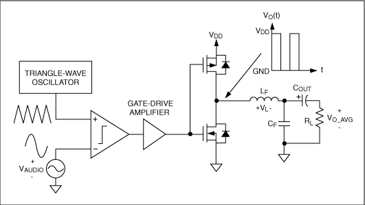
Figure 1. This simplified functional block diagram shows the structure of a basic half-bridge Class D amplifier.
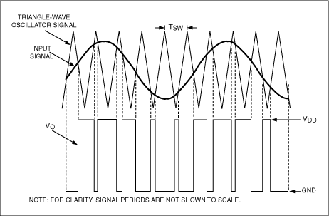
Figure 2. The output signal pulse width is proportional to the input signal amplitude.
In order to extract the amplified audio signal from the PWM waveform, the output of the Class D amplifier needs to be fed into a low-pass filter. The LC low-pass filter in Figure 1 acts as a passive integrator (assuming that the cut-off frequency of the filter is at least an order of magnitude lower than the switching frequency of the output stage), and its output is equal to the average value of the square wave. In addition, the low-pass filter prevents the dissipation of high-frequency switching energy on resistive loads. Assume that the filtered output voltage (VO_AVG) and current (IAVG) remain constant during a single switching cycle. This assumption is more accurate because fSW is much higher than the highest frequency of the audio input signal. Therefore, the relationship between the duty cycle and the filtered output voltage can be obtained by a simple time-domain analysis of the inductor voltage and current.
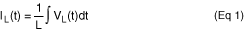
The instantaneous current flowing through the inductor is:
Among them, VL (t) is the instantaneous voltage of the inductor after using the symbol rule in FIG. 1.
Since the average current flowing into the load (IAVG) can be regarded as constant within a single switching cycle, the inductor current at the beginning of the switching cycle (TSW) must be the same as the inductor current at the end of the switching cycle, as shown in Figure 3.
With mathematical terms, it can be expressed by the following equation:
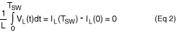
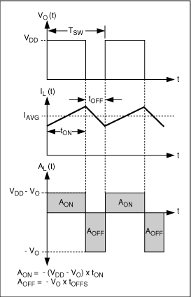
Figure 3. In the basic half-bridge Class D amplifier, the filter inductor current and voltage waveforms.
Equation 2 shows that the integral of the inductor voltage in one switching cycle must be zero. Using Equation 2 and observing the VL (t) waveform given in Figure 3, it can be seen that the absolute values ​​of the areas (AON and AOFF) of each region can only be established if they are equal to each other. Based on this information, we can use the switching waveform duty cycle to represent the filtered output voltage:
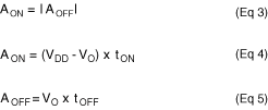
Substituting equations 4 and 5 into equation 3 yields the following equation:

Finally, get the expression of VO:
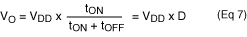
Where D is the duty cycle of the output switching waveform.
Using Feedback to Improve Performance Many Class D amplifiers use a negative feedback loop from the PWM output to the device input. The closed-loop scheme can not only improve the linearity of the device, but also make the device have power supply suppression capabilities. Open-loop amplifiers are the opposite. Their power-supply suppression capability is minimal (if any). In a closed-loop topology, the output waveform is detected and fed back to the input of the amplifier, so it is possible to detect the deviation of the power supply at the output and correct the output through the control loop. The advantages of closed-loop design come at the cost of possible stability problems, which is also a common problem faced by all feedback systems. Therefore, the control loop must be carefully designed and compensated to ensure stability under any operating conditions.
A typical Class D amplifier uses a feedback loop with noise shaping function, which can greatly reduce the in-band noise introduced by the non-linearity of the pulse width modulator, output stage, and power supply voltage deviation. This topology is similar to the noise shaping used in sigma-delta modulators. To illustrate the noise shaping function, Figure 4 shows a simplified block diagram of a first-order noise shaper. The feedback network usually includes a resistor divider network, but for simplicity, the feedback ratio in Figure 4 is 1. Since the gain of an ideal integrator is inversely proportional to frequency, the transfer function of the integrator in the figure is also simplified to 1 / s. It is also assumed that the PWM module has unity gain and zero phase offset in the control loop. Using the basic control module analysis method, the following output expressions can be obtained:
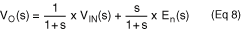
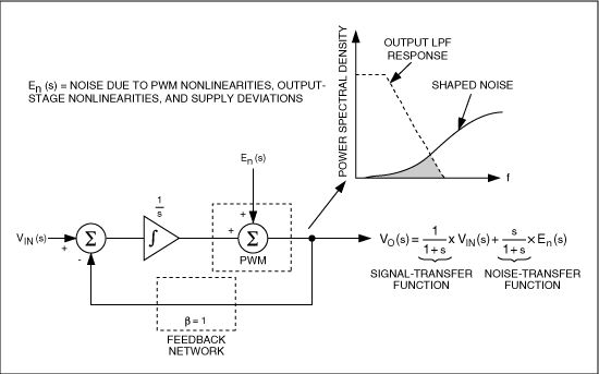
Figure 4. The control loop of a Class D amplifier includes a first-order noise shaping circuit that pushes most of the noise out of band.
As can be seen from Equation 8, the noise term En (s) is multiplied by a high-pass filter function (noise transfer function), and the input term VIN (s) is multiplied by a low-pass filter function (signal transfer function). The high-pass filter of the noise transfer function shapes the noise of the class D amplifier. If the cut-off frequency of the output filter is selected properly, most of the noise will be pushed out of band (Figure 4). The above example uses a first-order noise shaper, and most modern class-D amplifiers use a high-order noise-shaping topology to further optimize linearity and power supply rejection characteristics.
Class D topology—half bridge and full bridge Many Class D amplifiers also use full bridge output stages. A full bridge uses two half-bridge output stages and drives the load differentially. This type of load connection is commonly referred to as a bridge load (BTL). As shown in Figure 5, the full-bridge structure works by switching the conduction path of the load. Therefore, the load current can flow in both directions without a negative power supply or DC blocking capacitor.
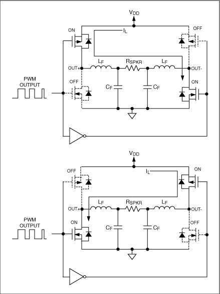
Figure 5. The traditional full-bridge class D output stage uses two half-bridge output stages to drive the load differentially.
Figure 6 shows the output waveform of a traditional, PWM-based BTL Class D amplifier. In Figure 6, the output waveforms are complementary to each other, thereby generating a differential PWM signal across the load. Similar to the half-bridge topology, an external LC filter is required at the output to extract low-frequency audio signals and prevent high-frequency energy from being dissipated on the load.
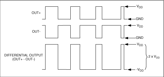
Figure 6. Traditional full-bridge Class D output waveforms are complementary to each other, generating a differential PWM signal across the load.
In addition to the same advantages as Class AB BTL amplifiers, full-bridge Class D amplifiers also have high efficiency characteristics. The first advantage of the BTL amplifier is that when using a single power supply, the output does not require DC blocking capacitors. This is not the case with a half-bridge amplifier, because its output swings between VDD and ground, with a 50% duty cycle when idle. This means that its output has a DC offset of about VDD / 2. In a full-bridge amplifier, this offset appears on both sides of the load, and the DC current at the output is zero. The second advantage they have is that at the same supply voltage, the output signal swing is twice that of a half-bridge amplifier because the load is driven differentially. Under the same power supply voltage, the maximum output power it can theoretically provide is four times that of a half-bridge amplifier.
However, the number of MOSFET switches required for a full-bridge class D amplifier is also twice that of a half-bridge topology. Some people think this is its disadvantage, because more switches means more conduction and switching losses. However, this is only true for high-power output amplifiers (> 10W) ​​because they require higher output current and supply voltage. In view of this, half-bridge amplifiers are often used in high-power applications due to their weak efficiency advantages. Most high-power full-bridge amplifiers have an efficiency between 80% and 88% when driving 8Ω loads. However, when each channel injects more than 14W of power into an 8Ω load, a half-bridge amplifier like the MAX9742 can achieve more than 90% efficiency.
Eliminate the output filter-filter-free modulator A major disadvantage of traditional Class D amplifiers is that it requires an external LC filter. This not only increases the total cost of the solution and board space, it may also introduce additional distortion due to the nonlinearity of the filter element. Fortunately, many modern Class D amplifiers use advanced "filter-free" modulation schemes, thereby eliminating or at least minimizing external filter requirements.
Figure 7 shows a simplified functional block diagram of the MAX9700 filter-free modulator topology. Unlike traditional PWM BTL amplifiers, each half-bridge has its own dedicated comparator, so that each output can be controlled independently. The modulator is driven by differential audio signals and high-frequency sawtooth waves. When both comparator outputs are low, each output of the Class D amplifier is high. At the same time, the output of the NOR gate becomes a high level, but there will be a certain delay due to the RC circuit composed of RON and CON. Once the NOR gate delay output exceeds a certain threshold, the switches SW1 and SW2 will close. This will cause OUT + and OUT- to go low and remain until the beginning of the next sampling cycle. This design makes the two outputs turn on simultaneously for a minimum time (tON (MIN)), which is determined by the values ​​of RON and CON. As shown in Figure 8, when the input is zero, the two outputs are in phase and have a pulse width of tON (MIN). As the audio input signal increases or decreases, one of the comparators will flip before the other. This operating characteristic, coupled with the effect of the shortest on-time circuit, will cause one output to change its pulse width and the pulse width of the other output to remain tON (MIN) (Figure 8). This means that the average value of each output contains the half-wave rectification result of the output audio signal. By performing a difference operation on the average value of the two outputs, a complete output audio waveform can be obtained.
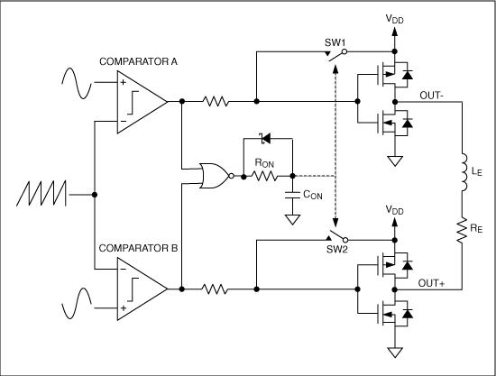
Figure 7. This simplified functional block diagram shows the topology of the MAX9700 filter-free Class D modulator.
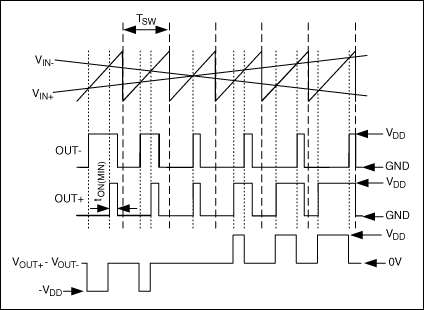
Figure 8. The input and output waveforms of the MAX9700 filter-free modulator topology.
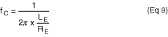
Because the output of the MAX9700 is a non-inverting signal when idle, there is no differential voltage across the load, which minimizes static power consumption and eliminates the need for external filters. Maxim's filter-free Class D amplifiers do not rely on external LC filters when extracting audio signals from the output, but rely on the inherent inductance of the speaker load and the auditory characteristics of the human ear to restore the audio signal. Loudspeaker resistance (RE) and inductance (LE) form a first-order low-pass filter whose cutoff frequency is:
For most speakers, this first-order roll-off is sufficient to restore the audio signal, and prevents excessive high-frequency switching energy from being dissipated in the speaker resistance. Even if the residual switching energy still causes the speaker assembly to move, these frequencies cannot be heard or affected by the human ear. When using a filter-free Class D amplifier, in order to obtain maximum output power, the speaker load should ensure that it is still an inductive load at the amplifier switching frequency.
Spread spectrum modulation minimizes EMI. A disadvantage of filter-free operation is the possibility of radiating EMI through speaker cables. Since the output waveform of the class D amplifier is a high-frequency square wave with a steep transition edge, the output spectrum will contain a large amount of spectral energy at the switching frequency and the switching frequency multiplier. If no external output filter is installed close to the device, these high-frequency energy will be radiated through the speaker cable. Maxim's filter-free Class D amplifier uses a patented spread-spectrum modulation * scheme to help mitigate possible EMI problems.
Spread spectrum modulation is achieved by jittering or randomizing the switching frequency of class D amplifiers. The actual switching frequency can vary up to ± 10% relative to the nominal switching frequency. Although each cycle of the switching waveform changes randomly, the duty cycle is not affected, so the output waveform can retain audio information. Figures 9a and 9b show the broadband output spectrum of the MAX9700, and the effect of spread spectrum modulation can be seen. Spread spectrum modulation effectively broadens the spectral energy of the output signal, rather than focusing the spectral energy on the switching frequency and its harmonics. In other words, the total energy of the output spectrum has not changed, just redistributed in a wider frequency band. This reduces the high frequency energy peak at the output, thus minimizing the chance of radiating EMI from the speaker cable. Although some spectral noise may be introduced into the audio bandwidth by spread spectrum modulation, these noises can be suppressed by the noise shaping function of the feedback loop.
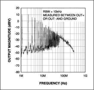
Figure 9a. Broadband output spectrum of the MAX9700 at a fixed switching frequency.
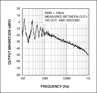
Figure 9b. Spread spectrum modulation distributes the spectral energy of the MAX9700 in a wider frequency band.
Many of Maxim's filter-free Class D amplifiers also allow the switching frequency to be synchronized to an external clock signal. Therefore, the user can set the amplifier switching frequency to a relatively insensitive frequency range.
Although spread-spectrum modulation greatly improves the EMI performance of filter-free Class D amplifiers, in order to meet FCC or CE emission standards, it is actually necessary to limit the length of the speaker cable. If the device fails the radiation test because the speaker cable is too long, an external output filter is required to attenuate the high-frequency components of the output waveform. For many applications with moderate speaker cable lengths, installing a bead / filter capacitor at the output will suffice. EMI performance is also very sensitive to layout. To ensure that the applicable FCC and CE standards are met, the PCB layout principles must be strictly followed.
Conclusion The latest developments in Class D modulator technology allow Class D amplifiers to flourish in applications where linear amplifiers once dominated. Modern Class D amplifiers have all the advantages of Class AB amplifiers (that is, good linearity and minimum board space), but also have high efficiency advantages. Currently, there are a variety of Class D amplifiers available to meet the needs of various applications. These applications include low-power portable applications (such as cellular phones and notebook computers), battery life, board space and EMI compatibility requirements are critical in such applications; also include high-power applications (such as car audio systems or flat panel displays ), To minimize heat dissipation requirements and heat generation is essential in such applications. A basic understanding of Class D amplifiers and their latest technological developments will help designers choose the right amplifier for a specific application and correctly weigh the advantages and disadvantages of certain functional features.
In the past, the typical class-D amplifier based on the PWM method required external filtering components, which would cause EMI / EMC compatibility problems, and the THD + N performance was poor. Therefore, its high-efficiency advantage was greatly lost compared with the linear amplifier. However, the latest generation of Class D amplifiers uses advanced modulation and feedback techniques to alleviate the above problems.
Basics of Class D Amplifiers Modern Class D amplifiers use a variety of modulator topologies, and the most basic topology combines pulse-width modulation (PWM) and triangular (or sawtooth) oscillators. Figure 1 shows a simplified block diagram of a PWM-based half-bridge Class D amplifier. It includes a pulse width modulator, two output MOSFETs, and an external low-pass filter (LF and CF) to recover the amplified audio signal. As shown in the figure, p-channel and n-channel MOSFETs are used as current steering switches, and their output nodes are alternately connected to VDD and ground. Because the output transistor switches the output between VDD and ground, the final output of the Class D amplifier is a high-frequency square wave. The switching frequency (fSW) of most Class D amplifiers is usually between 250kHz and 1.5MHz. The audio input signal performs pulse width modulation on the output square wave. The audio input signal is compared with the triangle wave (or sawtooth wave) generated by the internal oscillator to obtain a PWM signal. This modulation method is usually called "natural sampling", in which the triangular wave oscillator is used as the sampling clock. The duty cycle of the square wave is proportional to the input signal level. When there is no input signal, the duty cycle of the output waveform is 50%. Figure 2 shows the PWM output waveforms generated under different input signal levels.
Figure 1. This simplified functional block diagram shows the structure of a basic half-bridge Class D amplifier.
Figure 2. The output signal pulse width is proportional to the input signal amplitude.
In order to extract the amplified audio signal from the PWM waveform, the output of the Class D amplifier needs to be fed into a low-pass filter. The LC low-pass filter in Figure 1 acts as a passive integrator (assuming that the cut-off frequency of the filter is at least an order of magnitude lower than the switching frequency of the output stage), and its output is equal to the average value of the square wave. In addition, the low-pass filter prevents the dissipation of high-frequency switching energy on resistive loads. Assume that the filtered output voltage (VO_AVG) and current (IAVG) remain constant during a single switching cycle. This assumption is more accurate because fSW is much higher than the highest frequency of the audio input signal. Therefore, the relationship between the duty cycle and the filtered output voltage can be obtained by a simple time-domain analysis of the inductor voltage and current.
The instantaneous current flowing through the inductor is:
Among them, VL (t) is the instantaneous voltage of the inductor after using the symbol rule in FIG. 1.
Since the average current flowing into the load (IAVG) can be regarded as constant within a single switching cycle, the inductor current at the beginning of the switching cycle (TSW) must be the same as the inductor current at the end of the switching cycle, as shown in Figure 3.
With mathematical terms, it can be expressed by the following equation:
Figure 3. In the basic half-bridge Class D amplifier, the filter inductor current and voltage waveforms.
Equation 2 shows that the integral of the inductor voltage in one switching cycle must be zero. Using Equation 2 and observing the VL (t) waveform given in Figure 3, it can be seen that the absolute values ​​of the areas (AON and AOFF) of each region can only be established if they are equal to each other. Based on this information, we can use the switching waveform duty cycle to represent the filtered output voltage:
Substituting equations 4 and 5 into equation 3 yields the following equation:
Finally, get the expression of VO:
Where D is the duty cycle of the output switching waveform.
Using Feedback to Improve Performance Many Class D amplifiers use a negative feedback loop from the PWM output to the device input. The closed-loop scheme can not only improve the linearity of the device, but also make the device have power supply suppression capabilities. Open-loop amplifiers are the opposite. Their power-supply suppression capability is minimal (if any). In a closed-loop topology, the output waveform is detected and fed back to the input of the amplifier, so it is possible to detect the deviation of the power supply at the output and correct the output through the control loop. The advantages of closed-loop design come at the cost of possible stability problems, which is also a common problem faced by all feedback systems. Therefore, the control loop must be carefully designed and compensated to ensure stability under any operating conditions.
A typical Class D amplifier uses a feedback loop with noise shaping function, which can greatly reduce the in-band noise introduced by the non-linearity of the pulse width modulator, output stage, and power supply voltage deviation. This topology is similar to the noise shaping used in sigma-delta modulators. To illustrate the noise shaping function, Figure 4 shows a simplified block diagram of a first-order noise shaper. The feedback network usually includes a resistor divider network, but for simplicity, the feedback ratio in Figure 4 is 1. Since the gain of an ideal integrator is inversely proportional to frequency, the transfer function of the integrator in the figure is also simplified to 1 / s. It is also assumed that the PWM module has unity gain and zero phase offset in the control loop. Using the basic control module analysis method, the following output expressions can be obtained:
Figure 4. The control loop of a Class D amplifier includes a first-order noise shaping circuit that pushes most of the noise out of band.
As can be seen from Equation 8, the noise term En (s) is multiplied by a high-pass filter function (noise transfer function), and the input term VIN (s) is multiplied by a low-pass filter function (signal transfer function). The high-pass filter of the noise transfer function shapes the noise of the class D amplifier. If the cut-off frequency of the output filter is selected properly, most of the noise will be pushed out of band (Figure 4). The above example uses a first-order noise shaper, and most modern class-D amplifiers use a high-order noise-shaping topology to further optimize linearity and power supply rejection characteristics.
Class D topology—half bridge and full bridge Many Class D amplifiers also use full bridge output stages. A full bridge uses two half-bridge output stages and drives the load differentially. This type of load connection is commonly referred to as a bridge load (BTL). As shown in Figure 5, the full-bridge structure works by switching the conduction path of the load. Therefore, the load current can flow in both directions without a negative power supply or DC blocking capacitor.
Figure 5. The traditional full-bridge class D output stage uses two half-bridge output stages to drive the load differentially.
Figure 6 shows the output waveform of a traditional, PWM-based BTL Class D amplifier. In Figure 6, the output waveforms are complementary to each other, thereby generating a differential PWM signal across the load. Similar to the half-bridge topology, an external LC filter is required at the output to extract low-frequency audio signals and prevent high-frequency energy from being dissipated on the load.
Figure 6. Traditional full-bridge Class D output waveforms are complementary to each other, generating a differential PWM signal across the load.
In addition to the same advantages as Class AB BTL amplifiers, full-bridge Class D amplifiers also have high efficiency characteristics. The first advantage of the BTL amplifier is that when using a single power supply, the output does not require DC blocking capacitors. This is not the case with a half-bridge amplifier, because its output swings between VDD and ground, with a 50% duty cycle when idle. This means that its output has a DC offset of about VDD / 2. In a full-bridge amplifier, this offset appears on both sides of the load, and the DC current at the output is zero. The second advantage they have is that at the same supply voltage, the output signal swing is twice that of a half-bridge amplifier because the load is driven differentially. Under the same power supply voltage, the maximum output power it can theoretically provide is four times that of a half-bridge amplifier.
However, the number of MOSFET switches required for a full-bridge class D amplifier is also twice that of a half-bridge topology. Some people think this is its disadvantage, because more switches means more conduction and switching losses. However, this is only true for high-power output amplifiers (> 10W) ​​because they require higher output current and supply voltage. In view of this, half-bridge amplifiers are often used in high-power applications due to their weak efficiency advantages. Most high-power full-bridge amplifiers have an efficiency between 80% and 88% when driving 8Ω loads. However, when each channel injects more than 14W of power into an 8Ω load, a half-bridge amplifier like the MAX9742 can achieve more than 90% efficiency.
Eliminate the output filter-filter-free modulator A major disadvantage of traditional Class D amplifiers is that it requires an external LC filter. This not only increases the total cost of the solution and board space, it may also introduce additional distortion due to the nonlinearity of the filter element. Fortunately, many modern Class D amplifiers use advanced "filter-free" modulation schemes, thereby eliminating or at least minimizing external filter requirements.
Figure 7 shows a simplified functional block diagram of the MAX9700 filter-free modulator topology. Unlike traditional PWM BTL amplifiers, each half-bridge has its own dedicated comparator, so that each output can be controlled independently. The modulator is driven by differential audio signals and high-frequency sawtooth waves. When both comparator outputs are low, each output of the Class D amplifier is high. At the same time, the output of the NOR gate becomes a high level, but there will be a certain delay due to the RC circuit composed of RON and CON. Once the NOR gate delay output exceeds a certain threshold, the switches SW1 and SW2 will close. This will cause OUT + and OUT- to go low and remain until the beginning of the next sampling cycle. This design makes the two outputs turn on simultaneously for a minimum time (tON (MIN)), which is determined by the values ​​of RON and CON. As shown in Figure 8, when the input is zero, the two outputs are in phase and have a pulse width of tON (MIN). As the audio input signal increases or decreases, one of the comparators will flip before the other. This operating characteristic, coupled with the effect of the shortest on-time circuit, will cause one output to change its pulse width and the pulse width of the other output to remain tON (MIN) (Figure 8). This means that the average value of each output contains the half-wave rectification result of the output audio signal. By performing a difference operation on the average value of the two outputs, a complete output audio waveform can be obtained.
Figure 7. This simplified functional block diagram shows the topology of the MAX9700 filter-free Class D modulator.
Figure 8. The input and output waveforms of the MAX9700 filter-free modulator topology.
Because the output of the MAX9700 is a non-inverting signal when idle, there is no differential voltage across the load, which minimizes static power consumption and eliminates the need for external filters. Maxim's filter-free Class D amplifiers do not rely on external LC filters when extracting audio signals from the output, but rely on the inherent inductance of the speaker load and the auditory characteristics of the human ear to restore the audio signal. Loudspeaker resistance (RE) and inductance (LE) form a first-order low-pass filter whose cutoff frequency is:
For most speakers, this first-order roll-off is sufficient to restore the audio signal, and prevents excessive high-frequency switching energy from being dissipated in the speaker resistance. Even if the residual switching energy still causes the speaker assembly to move, these frequencies cannot be heard or affected by the human ear. When using a filter-free Class D amplifier, in order to obtain maximum output power, the speaker load should ensure that it is still an inductive load at the amplifier switching frequency.
Spread spectrum modulation minimizes EMI. A disadvantage of filter-free operation is the possibility of radiating EMI through speaker cables. Since the output waveform of the class D amplifier is a high-frequency square wave with a steep transition edge, the output spectrum will contain a large amount of spectral energy at the switching frequency and the switching frequency multiplier. If no external output filter is installed close to the device, these high-frequency energy will be radiated through the speaker cable. Maxim's filter-free Class D amplifier uses a patented spread-spectrum modulation * scheme to help mitigate possible EMI problems.
Spread spectrum modulation is achieved by jittering or randomizing the switching frequency of class D amplifiers. The actual switching frequency can vary up to ± 10% relative to the nominal switching frequency. Although each cycle of the switching waveform changes randomly, the duty cycle is not affected, so the output waveform can retain audio information. Figures 9a and 9b show the broadband output spectrum of the MAX9700, and the effect of spread spectrum modulation can be seen. Spread spectrum modulation effectively broadens the spectral energy of the output signal, rather than focusing the spectral energy on the switching frequency and its harmonics. In other words, the total energy of the output spectrum has not changed, just redistributed in a wider frequency band. This reduces the high frequency energy peak at the output, thus minimizing the chance of radiating EMI from the speaker cable. Although some spectral noise may be introduced into the audio bandwidth by spread spectrum modulation, these noises can be suppressed by the noise shaping function of the feedback loop.
Figure 9a. Broadband output spectrum of the MAX9700 at a fixed switching frequency.
Figure 9b. Spread spectrum modulation distributes the spectral energy of the MAX9700 in a wider frequency band.
Many of Maxim's filter-free Class D amplifiers also allow the switching frequency to be synchronized to an external clock signal. Therefore, the user can set the amplifier switching frequency to a relatively insensitive frequency range.
Although spread-spectrum modulation greatly improves the EMI performance of filter-free Class D amplifiers, in order to meet FCC or CE emission standards, it is actually necessary to limit the length of the speaker cable. If the device fails the radiation test because the speaker cable is too long, an external output filter is required to attenuate the high-frequency components of the output waveform. For many applications with moderate speaker cable lengths, installing a bead / filter capacitor at the output will suffice. EMI performance is also very sensitive to layout. To ensure that the applicable FCC and CE standards are met, the PCB layout principles must be strictly followed.
Conclusion The latest developments in Class D modulator technology allow Class D amplifiers to flourish in applications where linear amplifiers once dominated. Modern Class D amplifiers have all the advantages of Class AB amplifiers (that is, good linearity and minimum board space), but also have high efficiency advantages. Currently, there are a variety of Class D amplifiers available to meet the needs of various applications. These applications include low-power portable applications (such as cellular phones and notebook computers), battery life, board space and EMI compatibility requirements are critical in such applications; also include high-power applications (such as car audio systems or flat panel displays ), To minimize heat dissipation requirements and heat generation is essential in such applications. A basic understanding of Class D amplifiers and their latest technological developments will help designers choose the right amplifier for a specific application and correctly weigh the advantages and disadvantages of certain functional features.
Automatic Water Purifier,Electric Water Purifier,Low Cost Water Purifier,Household Water Purifier
JOYOUNG COMPANY LIMITED , https://www.globaljoyoung.com