
PDP Introduction 1. Introduction With the development of computer hardware and software and the rise of the Internet, major changes in human life styles have occurred, and the daily life of modern people can no longer be separated from displays. With appropriate information receivers (displays) and communication channels (wireless transmission and Internet), people's reach can be reached. This article will introduce you to the related technology of PDP, one of the displays.
Second, PDP principle and process introduction
(1) Light emitting principle
The luminous principle of PDP is the same as that of fluorescent lamps. Inert gas or mercury gas is injected into the vacuum glass, and then the voltage is applied to generate a plasma effect of the gas to emit ultraviolet light (UV light). When the fluorescent powder is distributed on the surface of the glass tube, the fluorescent powder will be excited to visible light, and the color of the visible light is determined by the type of fluorescent powder.
PDP displays can be imagined as hundreds of thousands of miniaturized fluorescent lamps gathered together to discharge, each discharge space is called a cell, and the gases enclosed in these discharge spaces are neon (Ne) and xenon (Xe ) Or helium (He) and xenon (Xe) and other types of inert mixed gas. These gases will produce a discharge phenomenon (plasma) under high voltage control, and the ultraviolet wavelength released by this discharge phenomenon is mainly 147 nanometers (nm). The phosphor coated on the inside of the discharge cell will emit visible light when excited by ultraviolet light with a wavelength of 147 nm. If it is a color PDP, the types of phosphors must include three different phosphors that can emit three primary colors of red (R), blue (B), and green (G), rather than a single phosphor that emits white light. The three kinds of phosphors are arranged in a linear shape or a mosaic shape. When a voltage is applied to the discharge cell, a discharge is caused. At this time, the generated ultraviolet rays irradiate the phosphor inside the cell to emit red (R) and blue (B ), Green (G) visible light of the three primary lights. Together with the design of the drive circuit and the image signal processing, the three primary colors of light can be mixed to produce a variety of colors to form a colorful picture.
(2) PDP basic structure The early development of PDP products can be simply divided into two types, DC type PDP and AC type PDP, according to the current limiting method or the voltage type applied during discharge. The DC type PDP starts the discharge with a direct current (DC) voltage and limits the size of its discharge current with a resistor. Therefore, there must be no dielectric (capacitor) layer in the structure, which prevents the accumulation of wall charges on the dielectric layer. So that it needs a higher starting discharge voltage. In order to reduce the starting voltage, an auxiliary anode and an auxiliary discharge channel are designed to assist the starting discharge; and in order to easily limit the discharge current to increase the life of the PDP, a resistive layer is designed. Therefore, the structure of the DC-type PDP is more complicated. On the other hand, the discharge electrode and the phosphor in the DC-type PDP structure are directly exposed in the discharge cell, so it is easy to be caused by the ion collision electrode in the plasma during gas discharge Damage and deterioration, thus reducing PDP life. In addition, the design of the resistance layer is difficult to achieve the same resistance in all cells in the panel in the actual process, and when the resistance difference is too large, it will cause the start of each cell The voltage is inconsistent. This makes it difficult to design circuits and effectively control the quality of products. In contrast, the AC PDP has a transparent dielectric layer and a protective layer (MgO layer) that is resistant to ion impact on the discharge electrode. Therefore, in order to initiate the discharge on the surface of the dielectric layer, the alternating current (AC) voltage is used to start the discharge, and because its electrode is covered with a protective layer that is resistant to ion impact, its life is longer than that of the DC type. Because AC-type PDP has the advantages of simple structure and long life, the current commercial PDP products are AC-type PDP as the mainstream. Therefore, the focus of the following discussion will mainly be AC ​​PDP.
(3) The basic structure of the AC-PDP basic process commercialized AC type PDP was established by Fujitsu in 1996, and its basic process can be simply divided into the upper board process and the lower board process, and the sealing and assembly process (Figure One). 
3.1 Upper board manufacturing process:
3.1 (a) Pattern production of transparent electrodes:
As shown in Fig. 1, in the upper plate manufacturing process, a transparent electrode is first made on the glass substrate. There are currently two types; ITO or SnO2. ITO or SnO2 differ in properties (Table 1). ITO has poor heat resistance and corrosion resistance and high cost, but has better light transmittance and conductivity. Generally, the manufacture of the whole-surface transparent electrode is made by glass manufacturers. If the process of the ITO conductive film is based on the physical sputtering method of the thin film process, then the ITO is etched to the required transparency by wet etching. Electrode pattern (Figure 2a). The SnO2 transparent electrode is mainly based on the CVD process, and its pattern is produced by a semiconductor lift-off process (Figure 2b), which needs to be manufactured by the panel manufacturer. This is an additional process for the panel manufacturer. Will cause trouble. Therefore, most PDP panel manufacturers mainly purchase ITO glass substrates and then etch ITO pattern. 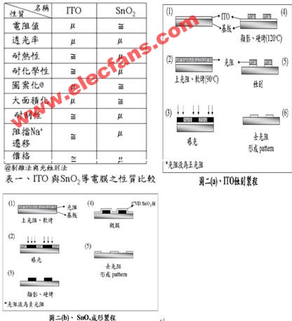
3.1 (b) Bus electrode production:
Because a large amount of heat is generated when the PDP panel generates plasma during discharge, the resistance of the transparent electrode becomes higher, which affects the voltage value of the gas discharge. In order to maintain a stable gas discharge voltage, a metal bus electrode is specially made on the transparent electrode layer to increase the conductivity. This metal bus electrode can be regarded as an auxiliary electrode. In the material structure, there are chromium / copper / chromium (Cr / Cu / Cr) or silver (Ag) electrodes. The former uses a thin-film process (sputtering or electron beam evaporation) to deposit three layers of metal on a substrate with a transparent electrode layer in sequence, and then the metal is etched in a wet etching process to complete the desired pattern (Figure 3). In the latter, the silver electrode paste is directly printed on the transparent electrode through a patterned screen by thick film printing. In addition to the above two methods, there are two other methods mainly based on wet etching. For example, DuPont developed a product called Fodel to make silver material into a strip-shaped photosensitive dry film, and pressed the dry film on the transparent electrode with a pressing machine, and then used a yellow light process to make it Etching into the desired pattern; the other is to make the silver electrode paste into a photosensitive paste, and print the entire surface of the material onto the glass substrate with the transparent electrode by printing, and then use the yellow light process Etch it to the desired pattern. 
The above four methods are adopted by different panel manufacturers. In terms of cost considerations, the first method: the process of plating Cr / Cu / Cr three-layer metal film and then etching is the highest, and the direct printing of silver electrode paste is the cheapest. Considering the precision of the pattern, the etching method is better than the printing method. At present, the manufacturing method of this bus electrode is mainly a photosensitive dry film for etching silver, because the pattern formed by this method has high precision and has been developed to recover silver waste after etching.
3.1 (c) Production of black contrast layer (black strip):
Early commercial PDPs had poor image contrast, so in order to improve this property, a black contrast layer was specially made next to the electrode on the upper plate. There are two ways to make this layer: one is to print the black paste by direct pattern printing; the other is to print the photosensitive paste and then etch into the desired pattern. The latter has higher precision.
3.1 (d) Transparent dielectric layer:
This layer is mainly printed by means of flat printing. The transparent dielectric glass material is printed on the entire surface of the electrode and the black contrast layer. At present, some manufacturers are actively studying the production of dry film. The requirements of this layer include its transparency must be more than 85%, the surface flatness should be less than 2mm, no bubbles should be generated and it should have high voltage resistance.
3.1 (e) Protective layer:
There are two main purposes of this layer. One is to prevent the ions in the plasma from hitting and etching the transparent dielectric layer and electrodes to increase the life of the PDP. The other is that the material itself has a high secondary electron emissivity , Can reduce the starting voltage during gas discharge. In addition, there are two requirements for this layer of material, one is that the transparency is high; the other is that this material itself can make the PDP panel have a wider operating voltage range. At present, various experimental studies have shown that MgO is one of the most resistant materials to ion impact and has high secondary electron emission efficiency and light transmittance (> 90%). Therefore, PDP uses MgO as a protective layer material, and its process is It is mainly based on the electron beam evaporation method in the film manufacturing process. At present, there is also research and development to produce MgO film with preferential orientation by ion-plaTIng.
3.2 Lower board process:
3.2 (a) Data (or address) electrode:
This layer uses silver as the electrode material. Generally, manufacturers usually print silver onto the glass substrate by a printing method. However, there are also research and development of photosensitive silver electrode materials, using yellow photolithography process to make Data electrodes. Although the resolution and yield of the Data electrode produced by the yellow photolithography process are very high, 50% of the silver material is wasted making the cost too high. Therefore, research is currently being conducted to save the cost by using recycled silver for reuse. In addition, there are also methods of making electrodes on glass substrates by electroless plating, but this method must pay attention to the problem of waste liquid treatment.
3.2 (b) White reflective dielectric layer:
The main purpose of this layer is to increase the reflection of visible light to increase the brightness and provide a flat surface with high flatness to reduce the difficulty of making the barrier wall. The current mass production method is mainly based on the printing method; there are also manufacturers that develop the white reflective dielectric layer into a dry film, and then use a laminator to laminate the reflection on the substrate.
3.2 (c) Barrier wall (rib):
This layer has two main purposes, one is to serve as a spacer between the upper and lower glass plates, and the other is to prevent the mixing of phosphors. However, with the user's requirements for the brightness and contrast of the PDP, the current barrier wall has been divided into two colors, the upper layer is black for the purpose of increasing the contrast of the picture; the lower layer is white for the purpose of increasing the brightness of the picture. Since the height of the barrier layer must reach 120-150mm and the flatness of the top of each barrier wall must be fairly consistent, it is currently the most difficult process and is a process that manufacturers actively want to develop and break through. The current mass production method uses sandblasting as the mainstream, but its shortcomings include: easy to cause dust, excessive material waste rate, holes on the surface of the barrier wall, and other methods such as printing or yellow light process must be used, so that the manufacturing cost is high. problem. Therefore, at present, various manufacturers are actively developing waste recycling after sandblasting or replacing the sandblasting method with a printing method to reduce manufacturing costs.
3.2 (d) Fluorescent layer:
This layer is coated between the two sides of the barrier wall and each barrier wall, and there should be no color mixing between adjacent two colors. This layer generally uses printing methods to fill different colors of fluorescent paste between the barrier walls, so it needs to be printed three times. In addition to printing, there are also studies on the use of photosensitive fluorescent pastes or dry films to make fluorescent layers, but ultimately, in consideration of cost, the main method is still printing.
3.3 Exhaust, inflation and sealing assembly process This process is to assemble the completed upper and lower plates according to the original design alignment marks and make a vacuum exhaust pipe, the sealing material used is low melting point ( 400 ~ 500oC) glass frit and apply this glass sealing layer on the periphery of the glass substrate with a glue coater. Then burn and fix the upper and lower plates together and complete the exhaust control process, followed by heating vacuum exhaust treatment. When the vacuum reaches a certain level, the appropriate amount of inert mixed gas is introduced. The components of this mixed gas are mostly He + Xe or Ne + Xe, and the mixing ratio and the enclosed volume are the secrets of each plant. The aging is performed after the sealing is completed, the purpose of which is to stabilize the characteristics of the discharge luminescence of each discharge space. After completion, the electrical and optical characteristics can be tested, and then through the electronic assembly and testing to complete the plasma display process. This process is currently the main bottleneck in mass production, and all equipment and mass production manufacturers are focusing on developing new equipment or improving this process.
Table 2 shows the requirements of material layers and their characteristics in the structure of PDP panels. Since various processes and materials of the PDP are still being continuously researched and improved in order to reduce the production cost and yield, we will not elaborate on the various processes here.

3.4 Drive circuit
The gray scale display of the PDP screen is controlled by its driving method. Therefore, the driving method will affect the quality of PDP products, so all manufacturers are actively developing their own driving methods. Generally speaking, the main driving method is to divide a frame into a fixed number of sub-fields, and then adjust the light-emitting time of each sub-field according to the needs of the frame to complete the gray scale representation. The main factors to be considered in designing the driving method include gas discharge characteristics, luminous efficiency, panel brightness and contrast, suppression of dynamic contours, power consumption, and heat dissipation. The early commercialized products are mainly based on the ADS (Address Display SeparaTIon: Address / Expression Separation Type) driving method published by Fujitsu. This method is not ideal for the processing of gray scale display and false contour. However, as consumers have higher and higher requirements for picture quality, various manufacturers are striving to develop more advanced driving methods to improve picture quality. For example, Fujitsu introduced the ALIS (Alternate LighTIng of Surface Method) drive method in 1998. This method not only improves the brightness, resolution and luminous efficiency of the picture, but also greatly reduces the power consumption and cost. However, this driving method must be coordinated with changes in the panel structure, so this driving method has become a feature of Fujitsu. Pioneer also released the CLEAR (Hi-Contrast & Low Energy Address & ReducTIon of False Contour Sequence) driving method. This method is characterized by improving the contrast of the picture, reducing the dynamic pseudo contour and luminous efficiency. The Matsushita Electric Industrial Co., Ltd. also proposed the Plasma AI driving method developed independently to improve the brightness and contrast of the screen and reduce power consumption. In addition to the above-mentioned companies, each company has also developed its own drive circuit to meet the characteristics of its own panel and to avoid the problem of patent rights.
3. In the future, any display product must be acceptable to the market. In addition to meeting basic functional needs, the most important thing is the rationalization of prices. Although the advantages of current PDP products are well understood by the general public and its picture effects (such as color temperature, brightness and contrast, etc.) are also close to the quality of CRT. However, when comparing the CRT with its price and quality, the PDP still has many areas to be improved. Therefore, the development direction of PDP commodities in the future should be carried out in two aspects; (1) low price, (2) performance improvement. Regarding lower prices, this can be achieved by lowering panel costs and reducing circuit costs. The former includes the development of new materials, new equipment, reduction of the number of processes, equipment and material standardization, and the improvement of the yield of mass production. Power recovery system, and low-cost driver IC. As far as performance improvement is concerned, it can be achieved by improving luminous efficiency and developing high-speed drive systems. The former includes the improvement of brightness and contrast, low power consumption and low starting voltage; the latter includes the improvement of animation quality, multi-grayscale and image reliability, etc.
In 1998, the 42-inch VGA-type PDP sold for about 360,000 TWD, and this year not only the quality has been greatly improved and the price has been reduced to about 200,000 TWD, but this price is still too high to attract ordinary household users to buy . Generally, Japanese manufacturers plan to reduce the price of PDP to NT $ 3000 for 1 inch in 2003, which means that the 42-inch VGA type PDP is about NT $ 130,000. At the current price reduction rate, this price target is likely Achieve in advance. Under the evaluation survey of the consumer market, the general household appliance industry generally believes that if the price of PDP products is less than 100,000 TWD, it can be quickly spread to ordinary households. In addition to the price and quality of PDP products, the achievement of PDP product penetration rate is also an important aspect of the cooperation of software, that is, the diversification of high-definition digital video content. However, digital video communication is an inevitable trend, and countries around the world are actively planning. Therefore, it is believed that in the near future, ordinary families can also use PDP products to enjoy high-quality digital multimedia programs.
Energy-saving Hospital Elevator
Bed Frame Elevators,Energy-Saving Elevator,Energy Efficient Elevators,Energy-Saving Hospital Elevator
XI'AN TYPICAL ELEVATOR CO., LTD , https://www.chinaxiantypical.com