
Commonly used active power factor correction circuits are classified into continuous current mode control type and discontinuous current mode control type. Among them, the continuous current mode control type mainly includes a boost type (Boost), a buck type (Buck), and a buck-boost type (Buck-Boost); the discontinuous current mode control type has a forward type (Forward) and a reverse type. The focus of the fly back, the following describes the working principle of these circuits.
1. Step-up PFC circuit
The main circuit of the step-up PFC is shown in Figure 1. The working process is as follows: When the switch Q is turned on, the current IL flows through the inductor L. Before the inductor is not saturated, the current increases linearly, and the electric energy is stored in the form of magnetic energy. In the inductor coil, at this time, the capacitor C discharge supplies energy to the load; when Q is turned off, the self-induced electromotive force VL is generated at both ends of L to keep the current direction unchanged. Thus, VL is in series with the power supply VIN to supply power to the capacitor and load.
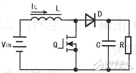
Figure 1 boost PFC main circuit
The advantages of this circuit are: (1) the input current is completely continuous, and can be modulated during the sinusoidal period of the entire input voltage, so that a high power factor can be obtained; (2) the inductor current is the input current, which is easy to adjust. (3) The gate drive signal of the switch tube is grounded with the output, and the drive is simple; (4) the input current is continuous, the current peak of the switch tube is small, and the adaptability to the input voltage is strong, which is suitable for the grid voltage change is particularly large. occasion. The main disadvantage is that the output voltage is relatively high, and the output short circuit protection cannot be realized by the switch tube.
2. Step-down PFC circuit
The step-down PFC circuit is shown in Figure 2. The working process is as follows: When the switch Q is turned on, the current IL flows through the inductor, and the current IL increases linearly before the inductor is saturated; when the switch Q is turned off , L generates self-induced electromotive force at both ends, and supplies power to the capacitor and the load. Since the converter output voltage is lower than the power supply voltage, it is called a buck converter.
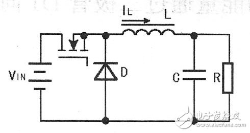
Figure 2 Step-down PFC main circuit
(1) The main advantage of this circuit is that the maximum voltage of the switch tube is the maximum value of the input voltage, so the voltage stress of the switch tube is small; when the rear stage is short-circuited, the output tube can be used for short-circuit protection.
(2) The main disadvantage of this circuit is that since the circuit can work only when the input voltage is higher than the output voltage, in each sinusoidal cycle, the circuit has a period due to the low input voltage and cannot work normally. The voltage is lower. At the same power level, the current stress of the DC/DC converter in the latter stage is larger; the gate drive signal of the switch tube is different from the output ground, the drive is more complicated, and the input current is interrupted, the power factor cannot be improved. A lot, so it is rarely used.
3. Lifting and pressing type PFC circuit
The buck-boost PFC circuit is shown in Figure 3. The working process is as follows: When the switch Q is turned on, the current IIN flows through the inductor, L stores energy, and the capacitor C discharges energy for the load; when Q is disconnected At the same time, IL has a decreasing trend, and the self-induced electromotive force generated in L causes diode D to be forward-biased, and L releases its stored energy to supply power to capacitor C and the load.
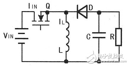
Figure 3 boost PFC main circuit
(1) The advantage of the circuit is that it can boost the input voltage and reduce the voltage, so it can work continuously throughout the input sinusoidal cycle; the output voltage selection range of the circuit is large, and can be designed according to different requirements of the first level; The output short circuit protection can be realized by using the switch tube.
(2) The main disadvantages of this circuit are: the voltage applied to the switching tube is the sum of the input voltage and the output voltage, so the voltage stress of the switching tube is large; since in each switching cycle, only when the switching tube is turned on There is input current, so the peak current is large; the gate drive signal of the switch tube is different from the output ground, and the drive is more complicated; the polarity of the output voltage is opposite to the polarity of the input voltage, and the inverter circuit of the latter stage is difficult to design, so it is also used. less.
Tip: Commonly used continuous current mode power factor correction chips are TDA16888 (PFC + PWM), 1PCS01 (PFC), L4981, FA4800 (PFC + PWM), UC3854, UCC3817, UCC3818 and so on.
4. Forward type PFC circuit
The forward-excited PFC circuit is shown in Figure 4. When the switching transistor Q is turned on, the diode D1 is forward-biased, the grid supplies energy to the load, and the output inductor L stores energy. When Q is turned off, the energy stored in L is released to the load through the freewheeling diode D2.
The advantage of this circuit is that the power stage circuit is simple, and the disadvantage is to add a magnetic reset loop to discharge the energy stored in the inductor during the forward period.
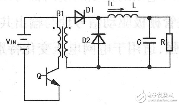
Figure 4 Forward PFC main circuit
5. Flyback PFC circuit
The flyback PFC circuit is shown in Figure 5. When the switch Q is turned on, the input voltage is applied to the primary winding of the high frequency transformer B1. Since the secondary side rectifier diode D1 is reversed, there is no current flow in the secondary winding. At this point, the capacitor C discharge supplies energy to the load. When the switch Q is turned off, the polarity of the voltage on the winding is reversed, the diode D1 is turned off, and the energy stored in the transformer is released to the load through the diode D1.
The advantage of this circuit is that the power stage circuit is simple and has overload protection.
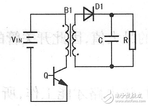
Figure 5 Flyback PFC main circuit
With the progress of science and technology, human beings are exploring step by step. As the carrier of Electronic Products, the technology of PCB Board is also more and more high-end. The design of PCB is more and more precise. Therefore, our production and processing also need improvement.
Now many research institutes in China have cooperated with us to discuss the contribution of PCB to the development of science and technology and to the human society.

Scientific Research PCB Board,Circuit Board Recycling,PCB Recycling,Printed Circuit Board Recycling
Orilind Limited Company , https://www.orilind.com