
0 Preface
TI's TMS320x family of DSPs is designed for real-time signal processing. This family of DSP controllers combines real-time processing power with controller peripheral functions to provide an ideal solution for control system applications. When designing a new type of metal detector, the author used the TMS320LF2407xA chip to analyze the AD sampling data, thus successfully controlling the motor operation.
The DSP chip TMS320LF2407XA has a 10-bit A/D converter inside. However, since it only contains a 10-bit A/D converter, if the first sign bit is removed, only nine bits are really useful, which does not meet the detection accuracy requirements of this project. To this end, this paper introduces a new method to improve the accuracy of DSP detection by an external 12-bit A/D converter (AD7858).
1 Main features of the AD7858
The AD7858 is a 12-bit serial, high speed, low power, successive approximation AD converter from AD. It operates from 3 to 5.5 V and has a data throughput rate of up to 200 kSPS. The chip contains a low noise, wideband track/hold amplifier that can handle wideband signals up to 200 kHz.
The AD7858 is easy to interface with a microprocessor or DSP. The input signal is sampled from the falling edge of CONVST (this bit can be operated by a hardware pin or software bit) and the conversion is also initiated from this point. The busy signal line is high at the start of the conversion and then transitions low after 400μs to indicate the end of the conversion.
The main features of the AD7858 are as follows:
â—‡ Supports 3 to 5.5 V voltage supply;
â—‡ Power-on system with automatic calibration (check chip itself or chip peripherals for errors) and automatic self-calibration (calibration
The function of whether the quasi register is wrong)
â—‡ has a high-speed serial interface;
â—‡ Low power consumption. At 3 V, the power consumption is only 12 mW;
A high-performance sample and hold amplifier is integrated into the chip. The input signal can be either single-ended or differential.
â—‡ AD7858 chip can support AD conversion by hardware or software;
◇The conversion is completed and automatically enters the sleep mode, and the power consumption during sleep is 25 μw;
â—‡ Available in a variety of packages such as 24-pin DIP, SOIC or TSSOP.
Figure 1 shows the internal functional block diagram of the AD7858.
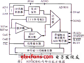
2 Pin Function of AD7858
The main pin functions of the AD7858 are as follows:
CONVST: Conversion start bit. When the falling edge of the clock comes, the system is in hold mode and begins digital to analog conversion. If this is not used, it should be connected to the DVDD;
BUSY: Busy signal output. Used to indicate the state the device is in. After the falling edge of CONVST or the rising edge of CAL, the busy signal goes high and remains high during the conversion. Once the conversion is complete and the conversion result is stored in the output register, the terminal is reset to low level;
SLEEP: Sleep or low power mode. When the pin is low, the device is in sleep mode. If there is no digital-to-analog conversion or calibration at this time, all circuits (including internal reference voltage) are in shutdown mode; if the pin is 1, the device is normal. run. If the sleep mode is only controlled by software, then this pin is always high;
REFIN/REFOUT: Reference input/output. This pin can be used as an internal reference voltage for analog-to-digital conversion and can be connected to internal circuits through series resistors;
AVDD: analog power terminal (3.0 ~ 5.5 V);
AGND: analog ground;
CREF1: Reference capacitor. This pin must be connected to a 0.01μF capacitor to the AGND pin;
CREF2: Reference capacitor. This pin must be connected to a 0.01 μF capacitor to the AGND pin;
AIN1-AIN8: Analog input. Can be used as single-ended input or differential input;
CAL: Verify input. This pin has an internal boost current of 0.15μA. In order to make the chip automatically self-calibration when powering up. This pin must be connected to the DGND pin with a 10 nF capacitor;
DVDD: digital power terminal (3.0 ~ 5.5 V);
DGND: digital ground;
DOUT: 16-bit serial data output;
DIN: 16-bit serial data input;
CLKIN: Digital clock input. The clock can determine the time of the digital to analog conversion;
SCLK: serial clock signal;
SYNC: Synchronization signal input. Active low.
Speakers with working frequency response range from 500~5000Hz are called mid range speakers.


FAQ
Q1. What is the MOQ?
XDEC: 2000pcs for one model.
Q2. What is the delivery lead time?
XDEC: 15 days for normal orders, 10 days for urgent orders.
Q3. What are the payment methods?
XDEC: T/T, PayPal, Western Union, Money Gram.
Q4. Can you offer samples for testing?
XDEC: Yes, we offer free samples.
Q5. How soon can you send samples?
XDEC: We can send samples in 3-5 days.
Mid Range Speaker
Mid Range Speaker,Mid Bass Speakers,Mid Range Car Speakers,Mid Bass Car Speakers
Shenzhen Xuanda Electronics Co., Ltd. , https://www.xdecspeaker.com