
With the development of railway transportation and the improvement of working and living conditions, the requirements of the working environment and conditions of the locomotive crew are getting higher and higher. Therefore, it is necessary to install an air conditioning system for the cab of the locomotive. However, since the air conditioning unit is a three-phase AC load, and the locomotive Power Supply is DC110V, it is necessary to design an inverter power supply, and convert the DC 110V into an AC 380v to supply the air conditioning unit.
Taking into account the particularity of the locomotive operating environment, such as: large vibration; high working environment temperature; frequent opening and closing of the door, making the air conditioning unit start and stop frequently; the driver's indoor electrical control equipment and signal equipment are dense, easy to generate mutual with the air conditioning power supply Electromagnetic interference, etc., therefore put forward higher requirements for the shock resistance, electromagnetic interference resistance, safety and reliability of the air conditioning power supply. According to the requirements of the technical indicators, within the range of ±30% of the control power supply and auxiliary input voltage fluctuations, the inverter power supply must provide voltage fluctuations of +1 0%/1 5% for the air conditioner, and the frequency fluctuation is within ±5%. The output voltage relative harmonic content (the ratio of the total rms value of the harmonic content below 3 1 and the total rms value of the output total voltage) is less than 5% of the three-phase 380V AC voltage, and is between 25 ° C and 70 ° C. Both can operate reliably.
2 working principle and hardware structure
It consists of a main circuit part and a control part. The boost chopper circuit is controlled by the PWM controller SG3525, and the inverter circuit is controlled by the single chip 87C196MC of the inte1 company.
2.1 main circuit
The main circuit of the inverter power supply is shown in Figure 2. It is mainly composed of DC/DC and DC/AC. The DC 1 1 0V input voltage is filtered by CI and sent to the boost circuit consisting of Ll, T1, and D7, and the voltage becomes DC 540V. The inverter circuit composed of VT 1 to VT 6 and D 1 to D 6 inverts the DC 540V voltage into three-phase AC 3 80V. The boost chopper circuit adopts the topology of the B00 St converter, and the switch tube uses an IGBT. The switching device of the inverter bridge uses the advanced intelligent power module IPM. IPM is based on IGBT as the basic power switching device, and integrates the function module of optimized gate drive and protection circuit. Its protection functions mainly include overcurrent, control power supply undervoltage and die overheating. When the module fails, the fault can be judged according to the output signal of the IPM fault output. The reliability of the system is further improved and the structure is more compact.
2.2 Control of the boost circuit
The boost circuit is controlled by a PWM controller SG 3 5 2 5 , and its peripheral circuit is shown in FIG. 3 . The SG3 525 is a voltage-type PWM controller that adjusts the output pulse width according to the feedback voltage. The internal is composed of a reference regulator, an oscillator, an error amplifier, a comparator, a PWM latch, an undervoltage lockout circuit, a flip-flop, or Non-gate, output stage, soft start and shutdown circuits.
After the circuit is powered up, the oscillator generates a continuous triangular wave with an amplitude between 1.2v and 3.6v and sends it to the PWM comparator inside the sG3525 chip, and simultaneously generates a synchronous square wave pulse for the T flip-flop to work.
   The isolated operational amplifier U1 (A7408) and the operational amplifier U2 (C40 74G) form a proportional integral (PI) regulator. The output voltage of the booster circuit is subjected to a voltage negative feedback signal through the PI regulator, and is input to the SG 3 5 2 5 internal error. The inverting input of the amplifier is compared with the reference voltage generated inside the chip of the non-inverting terminal, amplified, and output to the PWM comparator. Compared with the triangular wave of the oscillator, the output square wave is sent to the output pulse of the internal T flip-flop to The internal NOR gate of the chip alternately turns on the two output drive tubes to generate a switch control signal (1 1 or 14). The pulse width of the switch control signal is controlled by the voltage feedback signal. When the output voltage is higher than 540V, the voltage feedback signal that is isolated and amplified by the operational amplifier increases. Due to the negative feedback of the SG3525, the PWM pulse width of the output is reduced. The chopping output voltage is reduced; conversely, the SG 3 5 2 5 output PWM wave pulse width is increased, and the chopping output voltage is increased, so that the output voltage is maintained at 504 V.
Since the duty cycle of the PWM wave in the chopper circuit is about 0 to 8 4%. The duty cycle of the SG3525 single output can only reach 50% at most, so the two phases of the chip's 11 pin and 14 pin output are 180 out of each other. The PWM pulse is output to the switching tube of the booster circuit after the external NAND gate U3, which doubles the pulse frequency and satisfies the duty cycle requirement.
2.3 Inverter Controller 87C196MH
The inverter circuit uses Intel's 8 7 C 1 9 6 MC as the controller. 8 7 C 1 9 6 MC is a 16-bit MCU designed for three-phase AC induction motors and tributary brushless motors. It consists of a C1 96 core, an A/D converter, an event processing array EPA, two timings/ The counter, a three-phase waveform generator WFG, and a pulse width modulation unit PWM and seven I/O ports are formed.
The 87C1 96MC on-chip three-phase waveform generator WFG greatly simplifies the control software and external hardware used to generate synchronous PWM waves. The WFG has three synchronous PWM modules, each containing a phase compare register, a no-signal time generator, and a pair of programmable outputs to generate a complementary pair of PWM waves. Therefore, WFG can generate independent and non-overlapping three-phase six-way PWM waves with the same frequency and working mode, and output from P6 port, each driving current can reach 2 μA. In order to prevent the two switching tubes on the same bridge arm from being short-circuited at the same time, the dead zone interlock time can be set by the program to the WFG. When using the 16 MHz laser, the dead time can be set between 0.1 25 and 1 25 μs.
The hardware block diagram of the inverter control circuit is shown in Figure 4. The start-stop control circuit is the switch quantity control. When the start button is pressed, the chopper circuit works first. After the delay, the start signal is sent to the inverter control circuit, and the single-chip microcomputer starts to output the PWM pulse. When the inverter circuit generates an output overcurrent and an output phase loss, the fault feedback circuit causes the MCU to send a fault signal to the logic protection circuit, and uses the relay output. The external extended E2PROM is used as a data storage area to store several sinusoidal truth tables set according to different carrier ratios for the generation of SPWM waves. The Rs232 circuit is used to interface with the keyboard circuit. The protection circuit is provided with output overcurrent protection and phase loss protection circuit. The fault protection adopts the interrupt trigger mode. The overcurrent and phase loss protection signals are first connected to the P2 port, and then connected to the 87C196MH EXTINT via the AND gate, so that the CPU can be timely. Respond to the fault interrupt, judge the fault type according to the level change detected by the P2 port, so that the protection acts in time.
3 system software design 3.1 SPWH pulse width calculation
At present, the control algorithms for generating SPWM waves mainly include natural sampling method, symmetric rule sampling method, asymmetric rule sampling method, and area equivalent method. This design uses a symmetric regular sampling method with a triangular wave as the carrier and a sine wave as the modulated wave.
In the symmetric rule sampling method, the formula for calculating the pulse width is:
![]()
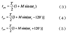
In the formula (2), Tt is a triangular wave period; M is a degree of modulation (O ≤ M < 1); ω is a sine wave frequency, and ts is a sampling time.
When the SPWM wave is generated by the WFG of the 87C196MC, the sine wave is first discretized according to the carrier ratio N, and the table is formed, and the half carrier period is also tabulated and stored in the E2PROM. In order to make the three-phase SPWM wave symmetrical, N should be an integer multiple of 3. Considering the elimination of harmonics, the larger N is better, but the value of N is limited by the switching frequency of the switching device and the operating speed of the microcontroller. By looking up the table and real-time calculation, the pulse width value is obtained and sent to the phase comparison register WG_COMPx. The value of WG_COMPx is compared with the 1/min 1 counter WG_COUNT after each count: WG_COUNT minus 1 is equal to WG_COMPx, and a trigger signal is output; after WG_COUNT is decremented by 1 to 0001H, 1 is added again, equal to WG_COMPx, and then output. A trigger signal, the time interval between the two trigger signals is the pulse width. The switching frequency is determined by the reload register WG_RELOAD.
The three-phase SPWM pulse width calculation formula is as follows:
The system software mainly consists of the system main sequence, EXTINT fault interrupt subroutine, WFG interrupt subroutine, A/D sampling interrupt subroutine.
The main functions of the main program are: initializing and parameter setting of each functional part of the single-chip microcomputer, detecting the state of the keyboard and button, sampling the input voltage and output current of the inverter circuit and judging whether the requirements are met, logic control and fault processing, calculating the modulation degree M Wait. The WFG interrupt subroutine is mainly used to generate the SPWM wave. The SPWM pulse width is calculated by the modulation degree M and the sine function table stored in the E2PROM, and the SPWM wave is generated. The EXTINT subroutine is mainly used for fault analysis and processing. When a fault occurs, it is determined by detecting different I/O ports, and the fault action is completed, such as fault alarm, blocking start pulse or tripping.
4 EHC design
In order to enable the locomotive to be powered reliably in harsh environments, reasonable and effective anti-jamming measures are essential.
In the hardware main circuit, the DC 11OV input voltage and the DC 540V chopping output voltage are filtered by capacitors to attenuate the noise generated from the external and chopper circuits. At the same time, the inverter circuit adopts the IPM module to make the structure compact. Reduced electromagnetic interference.
In the control circuit, a power supply filter is added to the power input end, and the power transformer is a shielded transformer. The ground of the control circuit is suspended, and is not shared with the main circuit, and the interface between the two is isolated by a high-speed optocoupler. The transmission line is twisted pair, and the signal line is kept as far as possible from the main circuit line of high voltage and high current. In the design of the printed circuit board, the interconnected devices are placed close to each other, and the components of the power circuit and the control circuit are separated as far as possible, and the input and output signals are placed as close as possible to the lead ports, and the power of each integrated chip is A CBB decoupling capacitor with a high frequency characteristic of 0.01 to 0.1 μF is connected between the ground.
5 Conclusion
It has been proved by experiments that the technical indicators of the power supply have reached the design requirements. It can be fully loaded and operated for a long time on the locomotive, which can meet the requirements of the rigorous operating conditions of the locomotive, and the work is stable and reliable.
:
MEAN WELL 15W--350W Enclosed-NE Series
Dual Voltage Variable 5Vdc 24Vdc,Nes-350-36,Mean Well 15W,Led Driver 5V
MEAN WELL LED Driver / LED Power Supply,MEAN WELL AC / DC Switching Power Supply Co., Ltd. , http://www.nbledpower.com