
This paper introduces a wireless remote control micro-shock motor vibration speed control circuit, which can complete the start, stop, acceleration and deceleration control of the motor speed in the wireless remote control mode.
Circuit principle
Micro-shock motor (also called hollow cup motor) has the characteristics of small size and obvious shock sense. The common shape is shown in Figure 1. There are many types of products on the market, all of which are driven by DC voltage. Take WZIS-6001A (B) type as an example, its characteristics are shown in Table 1. When the voltage of the motor changes from 2.0 to 3.8V, as the voltage increases, the motor speed gradually increases (from 7000 to 11,000 rpm). Through experimental tests, when the voltage changes by 0.3V, the speed of the motor can be felt by the vibration of the motor.
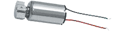
Figure 1 The appearance of micro-vibration motor

Divide the voltage range of 2.0 ~ 3.8V into 7 voltage gears, which are 2.0V, 2.3V, 2.6V, 2.9V, 3.2V, 3.5V, 3.8V. The rated current of the motor is 40mA, and a voltage difference of 0.3V can be generated by a resistance of 7.5Ω. See the corresponding dotted line in Figure 2. 74HC138 in the figure forms a 3-8 decoding circuit, which converts the 3-bit binary input of terminals A, B, and C into the decoding output of Y0 ~ Y7.
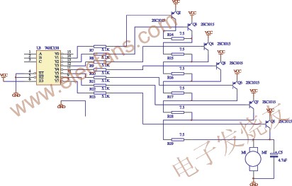
Figure 2 Motor speed gear control circuit
When A, B and C are 111, Y7 = 0, other Y0 ~ Y6 are 1, Q8 is turned on, Q2 ~ Q7 are turned off, the power supply VCC is added to the motor M1 through Q8, then the motor obtains the highest voltage and has the highest speed ;
When A, B and C are 001, Y1 = 0, the other Y0, Y2 ~ Y7 are 1, Q2 is turned on, Q3 ~ Q8 are turned off, the power supply VCC is added to the motor M1 via Q2, R14 ~ R19, then the motor obtains The lowest voltage with the lowest speed;
When A, B and C are 000, Y0 = 0, other Y1 ~ Y7 are 1, Q2 ~ Q8 are all cut off, and the motor stops running.
R7 ~ R13 in Fig. 2 constitute the base current limiting resistors of Q2 ~ Q8, Q2 ~ Q8 work in the switch working state, C5 is to eliminate the self-induction absorption capacitor of motor M1.
Remote control operation is converted into 74HC138 input A, B, C circuit
In order to realize the key control conversion into 74HC138 input A, B, C circuit in Figure 2, CD40193 constitutes a plus-minus bidirectional counter, CPU, CPD are the clock input ends of count-up and count-down, see the corresponding dotted line in Figure 3.
When the button S1 is pressed, A + is high, and when Q0, Q1, Q2 are not 1, the output of U2C is high, at this time CLK reaches the CPU end of U3 CD40193 via U2A as a binary count-up clock , And S2 is not pressed, A- is low level, CLK can not reach the CPD end of U3 CD40193 via U2B, then Q0, Q1, Q2 produce a binary count up from 000 to 111. When Q0 = A, Q1 = B, Q2 = C, the drive signal for the motor is gradually increased. Continue to press S1. When the count-up reaches Q0 = 1, Q1 = 1, Q2 = 1, the output of U2C is low. At this time, U2A prohibits CLK from passing, and its output is high. U3 CD40193 no longer counts up. The motor works at the highest speed, and the speed remains unchanged when you continue to press S1. At this time, the motor speed can only be changed by the S2 key operation.
When the button S2 is pressed, A- is high level, when Q0, Q1, Q2 are not 0, the output of U5A is high level, CLK reaches the CPD terminal of U3 CD40193 via U2B, as a binary countdown clock, Similarly, if S1 is not pressed, CLK cannot reach the CPU end of U3 CD40193 via U2C. The corresponding Q0, Q1, and Q2 generate a binary countdown from 111 to 000, which provides the motor with a gradually decreasing drive signal. When pressing S2 to Q0 = 0, Q1 = 0, Q2 = 0, U5A outputs low level in the same way, U2B prohibits CLK from passing, U3 CD40193 does not count down, the motor is stopped, and when S2 is continued, the motor remains at The stop state remains unchanged. At this time, the motor speed can only be changed by the S1 key operation. The function of R8 and C1 in the circuit is: at the moment when VCC is turned on, the capacitor C1 is too late to charge, so that the preset terminal PL of U3 CD40193 is low, and the preset number of P0, P1, P2, and P3 is asynchronously preset. To Q0, Q1, Q2, Q3. That is to ensure that when the power is turned on and there is no pressing action of S1 and S2, the motor will not malfunction.
CLK generating circuit
The CLK generating circuit is shown in the corresponding dotted line part in FIG. 3. When there is no key operation on S1 and S2, A + and A- are all low level, the input 5 pin of U4B is low level, so that its output is high level, then there is no clock pulse output of CLK, U3 of 1.2 above CD40193 will keep the output of Q0, Q1, Q2 unchanged, that is, the motor speed remains unchanged. When there is any key operation among S1 and S2, pin 5 of U4B is high, and the circuit generates a frequency of 1 / (1.4R5C2), that is, an oscillation clock output of about 2Hz, which provides up / down counting for the circuit of FIG. 3 Clock CLK. Among them, LED1 prompts the user for speed changes. Each time it flashes, it indicates that the speed increases or decreases by one level.
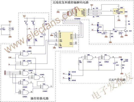
Figure 3 Operation conversion, CLK generated codec circuit
Wireless transceiver and remote control codec circuit
In order to realize the wireless remote control operation between the circuit of FIG. 2 and the circuit of FIG. 3, a wireless transmission and remote control coding circuit is introduced between Q0, Q1, Q2 to A, B, and C. See the corresponding dotted line in FIG. The remote control decoding circuit is shown in the corresponding dotted line part in FIG. 4.
In Figure 3, U1 SC2262 is a CMOS universal remote control encoder with the same function (reduce unnecessary pins) as PT2262, F05E is a power supply of 3 ~ 12V, including a sound meter resonator for frequency stabilization, and can work at 433MHz or 315MHz For the RF transmitter module, its 3-pin IN terminal trigger pole will not transmit when there is no input signal. When there is a signal input to its trigger, trigger emission is generated. Each trigger will output a series of pulse signals with a frequency of about 1kHz three times per second. The transmission distance can be improved by changing the R2 and F05E to increase the antenna, without increasing the antenna, and R2 = 47kΩ, the transmission distance can reach 12 ~ 15m. When R2 = 10kΩ, when the working frequency is 433MHz, when an 18cm enameled wire is added to the F05E as an antenna, the transmission distance can reach about 50m.
Among them, D1, D2, C4, C5, R3, R4, R11, Q1 constitute SC2262 code output effective control, when S1, S2 without key operation A +, A- is low level, Q1 does not conduct, SC2262 has no code Output; when there is a key operation, the key signal is processed by C4, C5, R4, R11 delay processing to turn on Q1, SC2262 encodes the input of Q0, Q1, Q2 and outputs to F05E for transmission. The purpose of C4, C5, R4, R11 delay is to eliminate the jitter of the button.
In Figure 4, J04V is a super regenerative RF receiving module, SC2272SML3 is a universal remote control decoding IC with the previous SC2262, which has the same function as PT2272ML; all contain D0, D1, D2 to keep the previous content when there is no new signal input at the DIN end change. J04V restores the received radio frequency signal to a data signal and sends it to SC2272SML3 for decoding to obtain the A, B, and C signals required by U3 74HC138 in Figure 2. R2, D7 are working indicator lights of the receiving circuit.
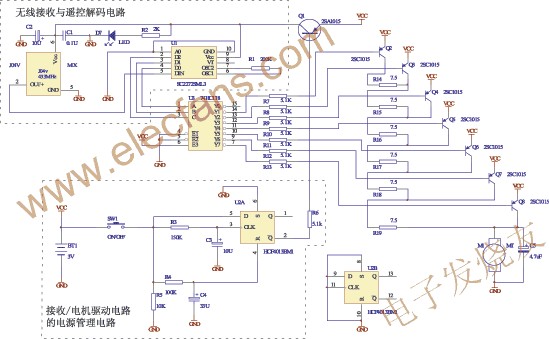
Figure 4 Wireless receiving and remote control decoding circuit, gear control circuit and power management circuit
Receiver / motor drive circuit power management circuit
The power management circuit of the receiving / motor driving circuit is shown in the corresponding dotted line part in FIG. 4. When SW1 is pressed, R3, C3 and R4, C4 form two integrating circuits. Known from the characteristics of the CD4000 series, when the potential of CLK (CD4013 PIN3) and R (CD4013 PIN4) rises to 1 / 2VCC, the output of CD4013 occurs change. The arrival time of the CLK terminal is t1 after SW1 is pressed, and the arrival time of the R terminal is t2 after SW1 is pressed. From FIG. 1, t1 = R3C3ln2 = 1 (s), t2 = R4C4ln2 = 2.29 (s) That is, when SW1 is pressed for time t: t1
Conclusion
The circuit can be applied to the vibrator circuit of medical acupuncture and moxibustion, and can also be applied to various health care electrotherapy equipment.
Brushless DC Motor,DC Brushless Motor,24V DC Brushless Motor,High Torque Brushless Motor
Changzhou Sherry International Trading Co., Ltd. , https://www.sherry-motor.com