
1 Introduction
Automatic test system ATS (AutomaTIc Test System) integrates all the excitation and measurement equipment required for testing. The computer efficiently completes the collection, storage and analysis of various modes of excitation and response signals, and performs automatic state monitoring, performance testing and Troubleshooting. The bus is an important part of the ATS, and is a common path for the computer and test hardware to transfer information inside and outside the peripherals. Its performance parameters directly affect the overall functional realization and performance indicators of the ATS.
Universal Serial Bus (Universal Serial Bus) is mainly used to interconnect PC and peripheral USB devices. Its physical connection is a layered daisy-chain structure that supports up to 5 Hub layers and 127 peripherals. The structure is highly independent. Strong anti-interference, high transmission rate, limited occupied resources, flexible use, and hot plugging support, so USB technology has gradually become the development trend of modern ATS data transmission.
Here, the high-speed data communication between the computer and the test control device FPGA and buffer FIFO is realized through the PE and GPIF interfaces of the Cypress USB microcontroller CY7C68013A. The ATS test command signal and data download, self-test and feedback data upload functions are implemented to realize the test technology. Intelligence. The emphasis is on the design of USB hardware and firmware code to explain the application of USB technology in the data transmission process of the test system.
2 USB interface communication workflow
USB has a flexible 1 two work flow, as shown in Figure 1.

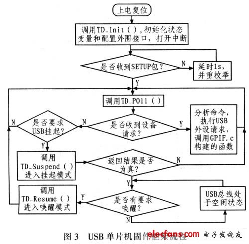
In Figure 1, the work flow of a USB device is from device connection → power on → reset → address assignment → configuration operation → execute firmware code, 6 working states, these states realize the transition between states and bus access under the control of USB host . The USB device judges whether to enter or exit the suspended state at any time according to the bus activity, saving the power consumption of the USB system.
From the analysis of Figure 1, we can see that USB communication includes USB system application software, devices and bus drivers and USB firmware 3 layers. Application software design consists of 2 parts: dynamic link library and application program. The dynamic link library is responsible for communicating with the kernel-mode USB function driver and receiving various operation requests of the application program for the USB device I / O. The application program calls the Win32 APl function DeviceToCon-trol to issue commands to the device; the USB device driver is driven through the bus The program issues an input and output request (IRP) to send and receive USB device information; the bus driver is responsible for bus detection, power management, and USB transaction processing; the firmware program implements the initial setting of the FX2 device, device request processing, power management, and peripheral Communication function is the core of the entire communication architecture. In the test system, the physical channel of data is established through the firmware code and the communication protocol is realized. The user can control the function of the USB device through the test software to realize the effective communication of data and complete the test task efficiently and reliably.
3 USB hardware circuit principle of the test system
CY7C68013A (referred to as 68013A) integrates USB2.0 transceiver, serial interface engine (SIE), enhanced 8051 core and programmable peripheral interface, provides an efficient USB2.0 solution, it can be configured for 3 data communication modes: port , GPIF and Slave FIFO modes. This design uses the features of GPIF mode such as fast and flexible to effectively solve the bottleneck of USB2.0 device data transmission speed in port mode, which greatly improves the data transmission rate. FX2 specifically provides peripheral interface signals for GPIF, such as 8 / 16-bit data lines, CTL, Ready signals and address lines. Considering the versatility, low power consumption, etc., the four I / O ports of PA, PB, PD and PE of 68013A, 6 CTL [5: 0] and 6 RDY [5: 0] are connected to FIFO or FPGA Realize data communication, handshake, control and other functions.
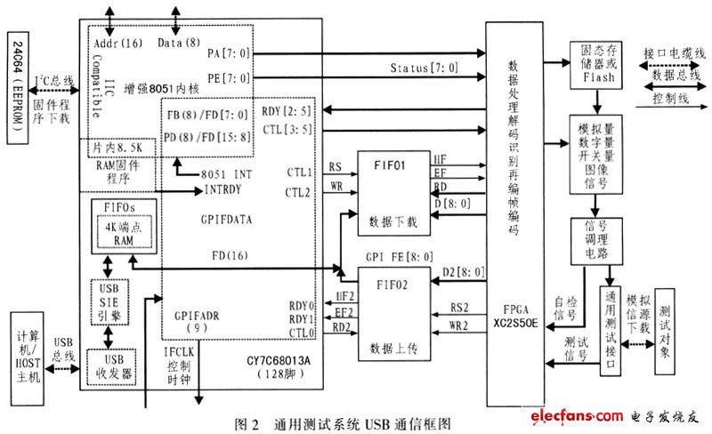
Figure 2 is a block diagram of GPIF hardware connection, where IFCLK is a bidirectional clock signal. When configured as an output, IFCLK is driven by FX2 to 30 MHz / 48 MHz: when configured as an input, the clock range is 5 to 48 MHz; GPIFADR (9) The signal provides an address line for external devices, and the address value on the bus is self-increasing; FD [15: 0] is the data line for the USB host to transfer data through FX2 and external devices, which can be configured as 8 or 16 bits; CTL [ 5: 0] is the peripheral control signal, such as read and write strobe, enable, etc .; RDY [5: 0] is the peripheral status detection signal, such as empty, full, etc. of the external FIFO.
The working principle of the entire system: the host downloads the corresponding test instructions and data to the 68013A internal FIFO through the USB bus through the application software settings, configures the relevant registers, ports and interrupts according to the same code to achieve data communication with the FIFO and FPGA. Two pieces of FIFO are used externally to match the data transmission rate. The external control signal RD (or RD2) / WR (or WR2) controls the reading / writing of data. In order to prevent the empty read or write overflow of the data, the FIFO status is marked with the flag terminals EF and HF. This internal and external FIFO double buffer design provides greater buffer space and timing matching for large-capacity, high-speed data transmission. While receiving data from the FIFO1, the FPGA determines the type and function of the received data according to the Status [7: 0] command received from the PE port, transmits the data to the corresponding test conditioning and output circuit, performs corresponding operations, and determines The working condition of the test object; if the self-inspection command is received from the PE port, the test data is collected to judge the working condition of the system itself. The signals fed back by the test object and the data collected by the test, the self-check data are processed by FPGA data fusion, and passed from FIFO2 to the GPIF receiving port of 68013A. All internal data and port operations of CY7C68013A are described by the firmware program.
Medium Voltage Motor Drive Solutions
8Pt Low Voltage Switch Cabinets,Low Voltage Switch Cabinet,Electric Motor Switchgear,Innovative Switchgear Solutions
Shandong Shunkai electrical equipment co., LTD. , https://www.chinasdsk.com