
In the early days of digital IC design (early 1960s), circuits were hand-made, and circuit diagrams (graphics) were hand-painted in paper, pen, and mimeographed. These circuit diagrams illustrate the logic gates and associated operational functions to build the design and its connections.
At least one member of each design team specializes in performing logic, minimizing, and optimizing, ultimately resulting in the replacement of a full group of gateways, performing the same work faster or taking up less silicon area.
Perform Functional Verification – Check that the design works as planned, usually by a group of engineers, sitting around the table and looking at the circuit diagram, saying, “Hey, I think it's okay!â€. Similarly, timing verification – checks if the design meets the required input/output and internal path delays, and does not violate any internal buffers (such as the setup and hold parameters) using pencil and paper.
Finally, the structure used to arrange the logical communication gates and the entire set of diagrams interconnected are all hand-painted. These are made up of simple graphics such as squares and rectangles, which are used to make photo-masks, and then the actual silicon chips are made using the mask.
The earliest digital ICs that are classified as "fully customized" according to today's terminology, because the dimensions and shapes of each of the geometric elements that make up an individual component are hand-painted separately. In order to solve the time-consuming and error-prone shortcomings, the schematic diagram (schemaTIc capture) package appears. Building digital designs at abstract communication gates is like creating software programs in assembly language.
In terms of performance and memory capacity, the combination process is called excellent build, but the capture and verification is time consuming and difficult to move to other computers for further development. Similarly, the fabrication and verification of the communication gate depiction is time consuming and not easy to move to a new fab or process.
Once the solution has to be transferred to a programming language such as C for higher-level development, high-level renderings are translated into machine language instructions required by the computer. The advantage is that software developers can quickly grasp the program's intent and then verify the functionality. In addition, programs written in C are easy to move to other computer platforms.
Once the digital logic designer begins to move to a higher-order abstraction of the so-called RTL (Register Transfer Level), the RTL depiction can be translated into a corresponding Logic synthesis technique that was introduced in the late 1980s and early 1990s. Communication gate circuit table (netlist). This "front-end" synthesis technology is enhanced by a "back-end" automated layout and place-and-route engine that can take the communication gate circuit table and perform design entity builds.
In small designs, the abstraction of the synthesis engine at the communication gate may not match the hand-painted design. However, in addition to quickly and succinctly grasping the design intent and greatly improving the productivity of the designer, the ability of the synthesis engine to automatically execute the speed and area trade-offs is better at expressing the overall performance of the synthetic engine.
Evolution of simulation tools
The development of computer-aided design and verification tools for analog circuits is much earlier than digital circuits. Design of individual components such as transistors, resistors, capacitors and inductors, etc., usually first establish a physical prototype of the design, then incorporate it into the test, measure the actual value to determine its performance, adjust the component values ​​and add/remove as necessary Components to achieve results.
In the late 1960s and early 1970s, many universities and commercial companies set out to develop analog simulators. These programs allow students and engineers to simulate the operation of analog circuits without having to actually build the circuit. The most famous early simulator was the SimulaTIon Program with Integrated Circuit Emphasis (SPICE) developed by the University of California, Berkeley, which was popular in the early 1970s.
In the past few years, the simulation simulator has made great progress in the evolution of basic models and algorithms, and the performance of simulation engines. Today's analog design and verification tools are basically limited by drawing and simulating transistor layer circuit diagrams.
• Delineate analog functions in a highly abstracted manner and then use these traces to create transistor layer equivalent circuits.
• Automatically optimize analog circuits.
• Automatic layout and winding analog circuits.
The result is analog integrated circuits, which are still mostly custom-made and require manual drawing. In addition to being expensive, time consuming, and erroneous, this transistor layer design approach does not allow existing designs to be easily transferred to new fabs or process/technical nodes. Instead, design migrations must begin with building circuits. This shows that the most advanced digital design has entered the 45nm technology, but the most advanced analog design is still at 90nm, and even many analog designs are still deep in the mud of 130nm and 250nm, and this It is technology 5 to 10 years ago.
Mixed signal instrument evolution
So far, the tools for truly mixed-signal solutions have progressed quite slowly. As mentioned earlier, in order to meet cost, size, weight and power consumption requirements, analog and digital functions will be combined on a single "mixed signal" device. Some EDA companies also try to "bolt together" existing simulations. With a digital simulation engine.
Traditionally, companies specializing in digital design have mostly tried to buy existing, mature analog solutions to solve problems. The motivation is to expand the market share by acquiring the customer base of the simulation company, but the result is still unable to integrate a large number of fragmented tools. Even with the contemporary "latest" mix of signals and a completely customizable design environment, the digital and analog design teams are still working, or even completely unaware of what the other party is doing. It is not uncommon for the personnel in the two fields to see each other for the first time when the chip is completed. At this time, the analog and digital blocks have already been laid out and wounded. However, the completion of the chip is usually done manually, including many of the work that takes place before the tape is put into production. Because of the lack of automation, the work and disposal of the chip is usually not able to be fed back to the main design process, leading to major problems in the future design. (This article is provided by MAGMA Product Manager)
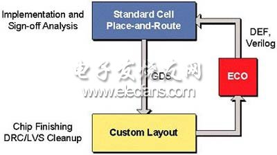
Caption: In traditional design environments, custom layouts and loops between standard cell layouts and windings can add weeks of chip development time.
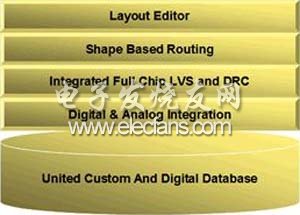
Caption: The TItan Chip Finishing system includes line layout editing software and a complete Quartz LVS verification solution.
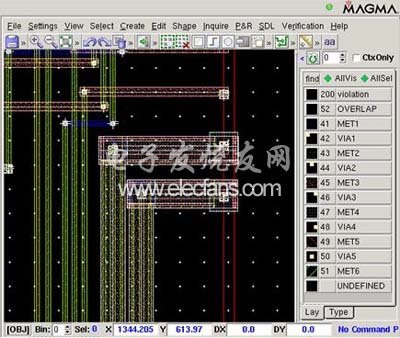
Caption: TItan Autoroute can increase productivity.
Stair Lights,LED Stair Lights,Stair Lights Indoor,Solar Step Lights
JIANGMEN LEDER LIGHTING CO., LTD , https://www.lederlight.com