
Abstract: A multi-channel video surveillance system is designed by using two dedicated video processing chips TMS320DM642 from TI. Among them, DSP1 and video acquisition chip SAA7113 jointly complete multi-channel video acquisition, and splicing into one video image output; DSP2 completes the acquisition, compression and video transmission of DSP1 output image. The scheme is flexible in structure and powerful in extension, and can realize real-time collection and transmission of 4-way video.
Keywords: video surveillance system; TMS320DM642; dual DSP; BT. 656
This article refers to the address: http://
Introduction In high-temperature and high-risk industries such as iron and steel smelting and processing, there are many occasions that are not suitable for workers to monitor the equipment on site for a long time. Therefore, it is necessary to establish an isolation studio on site and use the video surveillance system to collect and transmit real-time video from the scene to the studio. . In order to realize all-round equipment monitoring, multi-channel video surveillance system is often needed. In this paper, TI's dedicated video processing chip TMS320DM642 is used to build a single-channel multi-channel video surveillance system. The system is simple, convenient, and low in equipment cost, and can be widely used in field monitoring systems.
1 Core processor selection Video systems typically include the acquisition, processing, and output of video signals. The most central part is the processing part. For 4-channel 720×576 SD PAL video capture system and 1 720×576 SD PAL video output, the system input data is:
(720 × 576) × 4 × 16 bit × 25Hz ≈ 79.1 MB / s
The amount of output data is:
(720 × 576) × 16 bit × 25 Hz ≈ 19.8 MB / s
Dealing with such huge amounts of data has become the biggest bottleneck in multi-channel video surveillance systems. This requires the DSP to have a good external interface capability and a high core clock, use high-speed buffer devices and high-speed memory, and use a variety of techniques to complete the acquisition and processing of a large amount of video data.
TMS320DM642 (referred to as DM642) is a dedicated video processing chip introduced by TI. It is based on the C64X core, adopts VLIW (ultra-long instruction word) structure and L2 cache structure; the highest clock frequency is up to 720 MHz, and has a rich peripheral interface: 3 configurable video ports for video input/output Seamless connection; 64-way configurable EDMA for flexible data movement; 64-bit external memory interface (EMIFA) for simultaneous or asynchronous memory and peripherals; I2C bus interface for pairing Configuration of the external codec chip.
The DM642 has three configurable video port peripherals (VP0, VP1, VP2). Each video port has two channels, each of which can be seamlessly linked with a universal video encoder and decoder, supporting CCIR-601, ITU-BT. 656, BT. Video standards such as 1120. In this way, each DSP can be configured with 2 videos for video acquisition (ie, 4 channels are acquired simultaneously), and another video port is used for output display. In addition, the DM642 also has a 10/100M Ethernet interface for connection to external networks. Therefore, the DM642 is used as the main processing chip to realize the functions of video acquisition, compression and transmission. Considering that the system not only needs to collect multiple roadmap clear PAL video, it also needs to perform H. 264 compression coding, it is difficult to use a single DSP system to achieve real-time requirements, so the use of dual DSP systems. One DSP is responsible for acquisition and splicing, and the other DSP is responsible for video compression and transmission.
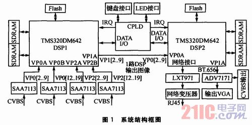
2 System overall design The system uses DM642 as the system core chip, and realizes the communication between DSPs by using the video port interconnection technology of DM642. At the video acquisition end, DSP1 and 4 SAA7113 form a 4-channel video acquisition system, and the video output port of DSP1 is connected to the video capture input port of DSP2. DSP2 mainly implements H.264 compression coding function in the system. The compressed data is sent to the general monitoring room through the network interface. In addition, the video port 2 of DSP2 is externally connected to the video coding chip to complete the output of analog CVBS and RGB format video data. The system structure block diagram is shown in Figure 1.
3 system hardware design
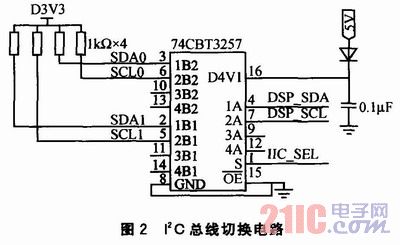
3.1 Video Decoding Module Design The video decoding module, also known as the video acquisition module, consists of a digital video decoding chip SAA7113 and a video source (analog CVBS signal). The input image is A/D converted by the video decoding module before it can be sent to the video processing module. The decoding module uses Philips' SAA7113 chip for acquisition. The analog CVBS signal output by the image sensor is converted into a digital signal by the SAA7113 video chip, and the output digital signal is buffered by the internal FIFO of the DM642 video port, by the DM642. The EDMA channel transfers data to off-chip SDRAM for use by video processing programs. The DM642 configures the SAA7113 through an I2C controller to output BT. 656 format 4:2:2 YUV video data stream.
It should be noted here that since the DM642 has only one I2C interface, it can only address up to two I2C slaves. In order to realize the configuration of the DM642 for four video decoding chips, the I2C bus is divided into I2C0 and I2C1 by using a multi-way selection switch 74CBT3257. The I2C bus switching circuit is shown in Figure 2.
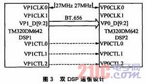
3.2 Dual DSP Communication Design The communication design of the dual DM642 can be implemented in two ways: dual port RAM and video port interconnection. The dual-port RAM adopts the shared memory mode, the system timing is complex, and the cost of the fast dual-port RAM is high. Therefore, the video port interconnection technology is adopted in the system to realize the dual DSP communication design.
The advantages of using video port interconnection technology are:
1 circuit design is simple, only 13 signal lines are needed to realize system communication, including 8 video port data lines, 2 clock lines and 3 optional control signal lines (field sync signals).
2DM642 video support BT. 656 format video output, while BT. The 656 format digital video embeds the sync signal in the data stream, eliminating the need for a line sync signal, which eliminates the need for additional chip-assisted control.
3 high transmission rate, up to 80 MB / s.
The design of the dual DSP communication module is shown in Figure 3. The system only needs to configure the video port 1 of DSP1 to display mode, then the VP1A will output the BT. The digital video data stream of the 656 format; at the same time, the video port 0 of the DSP2 is configured into an acquisition mode, and the BT of the DSP1 output is collected. 656 digital video stream, then deinterlaced and H. 264 compression processing. Due to BT. The 656 digital video stream has a sync signal embedded in it, so VPxCTL[O:2] can be connected.
3.3 Network interface module design The network interface module is mainly composed of DM642 Ethernet interface, network physical layer chip LXT971 and network transformer. Its main function is to compress and encode H. The 264 video data stream is transmitted to the general monitoring room. The LXT971 is a 10/100Base-TX Ethernet controller that is IEEE802.3 compliant and provides an MII interface for seamless connection to the MII interface of the DM642. The network transformer in the system uses 1:1 HR601680, its main function is to match the impedance, enhance the signal, increase the transmission distance and achieve voltage isolation. Since the UTP port of the LXT971 chip is current-driven, the center tap of the network transformer should be connected to the ground. The data transmitted from the DM642 is converted to the data that the Ethernet physical layer can receive by the LXT971, and then transmitted to the Ethernet through the RJ-45 interface via the network transformer.
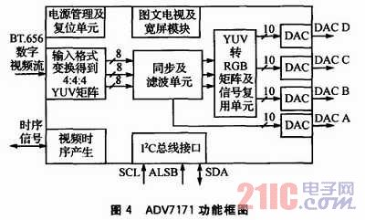
3.4 Video Encoding Module Design The video encoding module is also called the video display module. The ADV7171 is used to realize the video encoding function, and one CVBS and one VGA analog video output are obtained. The ADV7171 is a video encoder from Analog Devices that can be BT compliant. 656 and BT. The 601 format digital video is converted into CVBS composite video signal, analog RGB signal or S-Video signal output, and supports TV subtitles and teletext. Its functional block diagram is shown in Figure 4. VP1A output of DM642 BT. 656 digital video stream to ADV7171, ADV7171 completes the encoding and format conversion function and simultaneously outputs one CVBS signal and one RGB signal. At the same time, the ADV7171 is configured by the I2C interface of DM642.
3.5 Storage Space Expansion The DM642 uses storage mapping to organize storage space. The secondary cache map is mapped from 0x00000000 to 0x0003FFFF (256 KB total), and the external memory space is mapped in the address space after 0x80000 000. The external storage space is further divided into four independently addressable spaces, each of which occupies 256 MB from address 0x80000000. Each storage space corresponds to a CE space control register, and the memory type of each space is set by a register.
DM642 accesses off-chip memory through EMIF (External Memory Interface) memory interface. It integrates array bus, address bus, asynchronous control bus and SDRAM, SBS-RAM control bus, and supports memory seamless interface design such as SDRAM, SBSRAM and Flash. The space is configured to be 64-bit wide and used only for SDRAM memory mapping; the space is configured for 8-bit data width for Flash memory space expansion; it is not used in this design and is reserved for future expansion.
3.5.1 SDRAM Interface The EMIF interface of the DM642 has an SDRAM controller interface that enables seamless connection to SDRAM chips. The subspace is configured as a 64-bit SDRAM interface, and two 4M×32-bit SDRAMs are expanded into 4M×64 bits, and the specific address in the subspace is positioned as 0x80000000 to 0x81FFFFFF. SDRAM uses Hynix's HY57V283220 chip. It has 4 physical banks, each bank has a space of 1M×32 bits and a refresh period of 64 ms. It can read and write 1, 2, 4, 8 or full page data continuously or in an interleaved burst. The SDRAM operating clock is provided by the DSP's ECLK-OUT1 and can be configured by the AEA19 and AEA20 pins to be 1/4 or 1/6 of the EMIF CPU clock. SDRAM is mainly used to store a large amount of image data. Each chip requires 2 SDRAMs, and 2 DSPs require 4 SDRAMs. The SDRAM expansion schematic is slightly edited by the editor.
3.5.2 Flash Interface The external memory interface of the DM642 also provides an asynchronous interface for interfacing with a variety of memories and programmable external devices, such as SDRAM, E2PROM and Flash memory, as well as FPGAs, CPLDs, etc. The system is configured with a 4M x 8-bit Flash for each DSP to cure the program and initialize the data. After the system is powered on or reset, load the program and data from the 0x00000000 of Flash to the SDRAM space. The DSP configures the EMIF space as an 8-bit asynchronous static memory Flash interface. Flash uses the 90 ns AM29LV320DT with 22 address lines. Since the external address bus of the DM642 is only A[22:3], the maximum addressing range of the subspace is 1M×8 bits. In addition to being allocated to the Flash space, the CE1 subspace is also allocated to resources such as status/control registers. Flash only occupies half of the addressing space of the CE1 subspace. The maximum addressable range is 512K×8 bits, and the design capacity of Flash is 4M × 8 bits. In order to access the entire Flash space, Flash needs to be paged, each page is 512 KB, which is divided into 8 pages. The page addresses PA20, PA19, PA18 and Flash chip select signals are all from CPLD. Flash interface circuit slightly - editor's note.
4 PCB Circuit Design The DM642 has a core clock of 720 MHz and an SDRAM bus speed of 133 MHz. The system is a high-speed signal circuit. In order to ensure the normal operation of the system, it is necessary to consider the problems of transmission line effect, signal integrity, power integrity and electromagnetic compatibility, and use high-speed circuit wiring knowledge to design impedance matching and stack structure, and to ensure a good power supply system.
First, a good laminate design is the key to ensuring the signal integrity and power integrity of the system, while a good laminate design also contributes to the routing of the circuit. The system adopts an 8-layer circuit structure, and the 8-layer board layer structure is a signal layer 1 a ground layer a signal layer 2 a power layer 1 a ground layer a signal layer 3 a ground layer a signal layer 4 , wherein the signal layer 1 and the signal layer 4 The top layer and the Bottom layer are respectively. Such a laminate design allows the power layer to be in close proximity to the ground plane to ensure the integrity of the system power supply design; at the same time, the ground layer between the signal layers effectively isolates the four signal layers, causing crosstalk between the signal lines between the signal layers. Minimize to ensure the return path of the signal to ensure the signal integrity of the system.
Second, impedance matching must be performed on the high-speed bus signals in the system to reduce signal reflection and signal overshoot. Common matching networks include serial termination and AC parallel termination. Considering the influence of PCB layout space, bus signals are generally terminated by resistor serial termination, while analog video signal lines are connected by AC parallel termination. In the system design phase, the pre-layout simulation can be performed using the HyperLynx simulation software based on the IBIS model to determine the impedance matching network and the wiring width. The bus system uses a 33 Ω serial termination, while the analog video signal line uses a 75 Ω AC parallel termination network.
Finally, the system's power plane and ground are split and effectively bypass the ground and bounce noise on the power supply, adding decoupling capacitors where appropriate. The decoupling capacitors should be distributed as close as possible to the decoupling chip while trying to evenly distribute a capacitor across each supply pin.
Since the system is a high-speed signal processing system, HyperLynx can be used for pre-layout simulation before wiring, especially for the storage modules and network differential modules in the system to determine the impedance matching network and the wiring width. After the wiring is completed, post-layout simulation can also be performed to ensure the signal integrity of the system and reduce the electromagnetic interference of the system.
Conclusion This system uses TI's dedicated video processing chip TMS320DM642 to complete the design of dual DSP multi-channel video surveillance system. Compared with the traditional multi-channel video surveillance system, the multi-channel video surveillance system with dual DSP is simple in design and low in development cost, and can be widely used in the field of industrial field monitoring such as coal and steel.
11Kv Transformer,11Kv Dry Type Transformer,11Kv Cast-Resin Transformer,2500Kva Dry-Type Transformer
Hangzhou Qiantang River Electric Group Co., Ltd.(QRE) , http://www.qretransformer.com