
K9F6408U0A is a non-type 64 Mbit flash memory produced by Samsung. It has the advantages of low operating voltage, fast erasing speed and small size. SPDS202A's voice chip produced by Taiwan's Lingyang Company. The paper introduces the digital recording system with SPDS202A as the core, and introduces the specific method of realizing the copy function between two K9F6408U0A. Finally, the relevant hardware interfaces and software programs are given.
This article refers to the address: http://
1 K9F6408U0A performance brief
The biggest advantage of the K9F6408U0A is that its commands, data, and addresses can communicate with the host controller through eight I/O lines. This greatly simplifies the connection of the system and enhances the stability of the system. In addition to the eight I/O lines, the K9F6408U0A also includes the following control lines, which makes it easy to control the K9F6408U0A from the system's main controller. They are:
CLE: Command latch enable, active high. On the rising edge of the WE signal, the command signal can be locked into the command register via the I/O port.
ALE: Address latch enable, active high. On the rising edge of the WE signal, the address signal can be latched into the address register via the I/O port.
CE: Chip select line, active low. The CE high level is ignored during page programming or block erase operations or when the device is busy.
WE: Write enable port, command, address and data are locked on the rising edge of the WE signal.
RE: Read the enable port, send data to the I/O line on the falling edge of the port, and increment the internal column address register by one.
WP: Write protection port, active low. When it is low, the program and erase operations are disabled.
R/B: Operation status indication signal. When low, it indicates that a program is being programmed, erased or read, and becomes high after the operation ends.
2 Introduction to SPDS202A
SPDS202A is a cost-effective voice chip produced by Taiwan SUNPLUS Company. It can interface with the host very conveniently. The host can control the recording and playback functions of the voice chip by issuing command codes. It has the following characteristics:
â— For single-chip audio/speech coding/* chips, use SACM-S480 or SACM-S3200 compression and decompression algorithms. With a sampling rate of 8 kHz, the data low code rate is 4.8 kbps or 32 kbps;
â—With digital volume control function;
â— With FLASH management function, it can automatically manage FLASH data internally. Its standard FLASH interface can connect up to 4 FLASH, a total of 64Mbit.
â—Using the UART interface, it can easily interface with PCs and other RS232 devices, and can easily upload or download data.
â— embedded phase-locked loop circuit;
â— Embedded high quality 10-bit 8kHz ADC and DAC;
â— Low power consumption, using 2.8V ~ 3.6V operating voltage.
Due to the above characteristics of the SPDS202A, a large-capacity voice recording and playback system can be constructed by adding a small number of peripheral circuits.
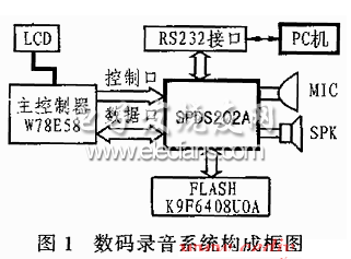
3 The composition of the digital recording system
The structure of the digital recording system with the SPDS202A as the core and the Winbond W78E58 as the main controller is shown in Figure 1. The W78E58 is compatible with the MCS-51 series of microcontrollers. Its built-in 32kflash EEPROM can be used as program memory, while the built-in 256 The byte SRAM is well suited for the magnetic programming operation of the K9F6408U0A.
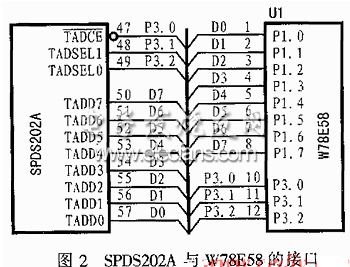
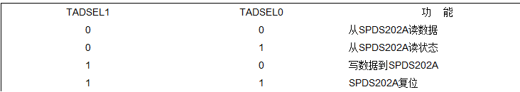
Figure 2 shows the W78E58 and SPDS202A hardware interface circuits. In the figure, TADCE is a chip select signal line that can latch commands/data on its rising edge. TADSEL1 and TADSEL0 are command selection signal lines, and their functions are listed in Table 1. Table 1 Command selection signal line function
TADD7~TADD0 are 8-bit data lines. When it is working, the main controller's SPDS202A sends three bytes of data, where the first byte is always 0FFh, the second byte is the command code low byte, and the third byte is the command code high word. The two bytes of data returned from the SPDS 202A are then received by the primary controller. The communication procedure between the two is as follows (written in C51):
Void Mcu_202_Comm(void) /*MUC and SPDS202A communication program*/
{via=0xFF; /*The first byte is sent to 0FFh*/
SendOneData( ); /* call to send a one-byte data subroutine*/
Via=CMDL; /* The second byte sends the command code low byte*/
SendOneData( );
Via_CMDH; / * third byte to send command code high byte * /
SendOneData( );
ECHOL=ReadOneData( ); /*Read return data*/
ECHOH=ReadOneData( );
}
The following is an example of the implementation of the recording function, which clearly shows how the system works.
Void Record(void)
{CMDL=0x00; /*Send recording command code*/
CMDH = 0x10;
Mcu_202_Comm( );
If(Err=1) /* If an error occurs, it returns */
{Err=0;
Return;
}
}
It can be seen that the system implements its function by sending a series of control command codes to the SPDS 202A through the main controller.
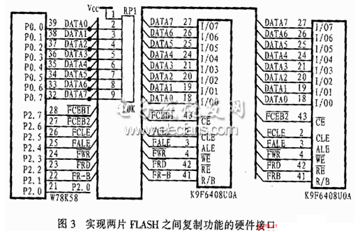
4 implementation of the copy function
In order to be able to save and back up the recorded information, you should consider implementing a copy function that copies the information on one K9F6408U0A to another. The hardware interface circuit that implements this function is shown in Figure 3. In the figure, the two K9F6408U0A are separated by the chip selection line, and the other signal lines are multiplexed. The copy function can be implemented using the following procedure:
Void Copy(void)
{FCEB2=1;
FCEB1=0; /*Select the first FLASH*/
For (RowAdd2=0; RowAdd2<64; RowAdd2+ +)
{for(RowAdd1=0; RowAdd1<256; RowAdd1+ +)
{BlockErase ( );} /* Call the block erase sub-function to erase the first FLASH content */
}
For(F1RowAdd2=0, F2RowAdd2=0; (F1RowAdd2<64)
(F2RowAdd2<64); F1RowAdd2+ +,
F2RowAdd2+ +)
For (F1RowAdd1=0, F2RowAdd1=0;
(F1RowAdd1<256) (F2RowAdd2<256);
F1RowAdd1+ +, F2RowAdd1+ +)
For (F1ColAdd=0, F2ColAdd=0; (F1ColAdd<256) (F2ColAdd<256); F1ColAdd=F1COAdd+128; F2ColAdd=F2ColAdd+128)
{CE1=1;
CE2=0;
SetPointer=0x00;
F1RdData( ); /* calls read data subfunction from the first FLASH */
CE2=1;
CE1=0;
SendData( );/* calls to send data sub-function to the second FLASH page register */
CE1=1;
CE2=0;
SetPointer=0x01; /* set page register pointer to the second half of the page register */
F1RdData( );
CE1=1;
CE2=0;
SendData( );
FwrData( ); /* Execute page programming command to write data to the second FLASH*/
}
}
}
}
5 Conclusion
The digital recording system records up to 3.7 hours of voice information on a 64Mbit FLASH. At the same time, in order to be able to save the recorded information, a copy between the two FLASHs can also be implemented using the copy method described herein. The system can be widely used in applications where long-term voice recording is required.
Pc Power Supply,Gold Pc Power Supply,Desktop Power Supply 650W,Psu Computer Power
Boluo Xurong Electronics Co., Ltd. , https://www.greenleaf-pc.com