
Gallium nitride (GaN) power semiconductor technology has made a significant contribution to improving the performance level of RF/microwave power amplification. By reducing parasitic components of the device, as well as using shorter gate lengths and higher operating voltages, GaN transistors have achieved higher output power density, wider bandwidth, and better DC-to-RF efficiency. For example, in 2014, a radar system application based on GaN-based X-band amplifiers was demonstrated, which provides 8 kW of pulse output power to replace traveling wave tube (TWT) devices and TWT amplifiers. The 32kW version of these solid state GaN power amplifiers is expected to appear in 2016. While looking forward to these amplifiers, we will examine some of the key features and characteristics of high power GaN amplifiers.
Not long ago, GaN was the technology of choice for Reflective Frequency Electronic Warfare (CREW) applications, and thousands of amplifiers have been delivered for practical use. Now, the technology is also deployed in the field of airborne electronic warfare, with amplifiers under development capable of delivering hundreds of watts of output power over multiple octaves in the RF/microwave range. Multiple versions of such broadband electronic warfare power amplifiers will be released this year.
Subsequent research includes improved linearity of peak-to-average power ratio (PAPR) waveforms used in many military communications systems, including general data link (CDL), broadband network waveform (WNW), soldier radio waveform (SRW), and broadband. Satellite communication (satcom) application. ADI's "Bit to RF" program will integrate the company's strengths in baseband signal processing and GaN power amplifier (PA) technology. By using techniques such as pre-distortion and envelope modulation, this integration will help improve PA linearity and efficiency.
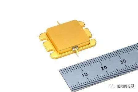
GaN devices released in the past few years have both discrete field effect transistors (FETs) and single-chip microwave integrated circuits (MMICs), which have been widely used in high power microwave amplifier systems. These devices are available from a number of fab and device manufacturers and are typically fabricated on 100mm silicon carbide (SiC) wafers. The GaN process on silicon is also being considered, but the thermal conductivity and conductivity of silicon are relatively poor, offsetting its cost advantage in high performance, high reliability applications. These devices feature gate lengths as small as 0.2μm and support operation in the millimeter wave band. In many high frequency applications and in all low frequency applications (except for the most cost sensitive applications), GaN-based devices have largely replaced gallium arsenide (GaAs) and silicon laterally diffused metal oxide semiconductors (LDMOS). ) device.

RF power amplifier designers are concerned with GaN devices because they support very high operating voltages (three to five times higher than GaAs) and that the gate width per unit FET allows approximately twice as much current as GaAs devices. These characteristics are important to PA designers, meaning that higher load impedances can be supported at a given output power level. Previous output designs based on GaAs or LDMOS are often extremely low (relative to typical system impedance of 50 Ω or 75 Ω). Low device impedance limits the achievable bandwidth, that is, as the impedance conversion ratio between the amplifier component and its load increases, the component count and insertion loss increase. Because of this high impedance, early adopters of such devices in some cases installed only one device in a mismatched test fixture, applied a DC bias, and driven the device with an RF/microwave test signal. Results.
Due to these operating characteristics and their exceptionally high reliability, GaN devices are also suitable for high reliability space applications. Life testing of multiple device vendors at junction temperatures of 225 ° C or higher showed that the average pre-failure time (MTTF) of a single device exceeded one million hours. This high reliability is mainly due to the high bandgap value of GaN (3.4 for GaN and 1.4 for GaAs), which makes it particularly suitable for high reliability applications.
The main obstacle to expanding the use of GaN in high-power applications is that it is relatively expensive to manufacture, typically two to three times higher than GaAs, and five to seven times higher than Si LDMOS devices. This has hampered its use in cost-sensitive applications such as wireless infrastructure and consumer handheld devices. Now with the GaN process on silicon, despite the performance issues mentioned above, devices produced by this process may be best suited for cost-sensitive applications. In the near future, as GaN device manufacturing shifts to larger-sized wafers (150mm in diameter and larger, and many leading GaN device foundries are currently being developed), the cost is expected to decrease by about 50%.
Currently deployed radar systems for weather forecasting and target acquisition/recognition rely on TWT power amplifiers operating at C-band and X-band frequencies. These amplifiers operate at high supply voltages (10 kV to 100 kV) and high temperatures and are susceptible to damage due to excessive shock and vibration. The field reliability of these TWT amplifiers is typically only 1200 to 1500 hours, resulting in high maintenance and spare parts costs.
As an alternative to high-power TWT amplifiers, Analog Devices has developed an 8kW solid-state X-band power amplifier based on GaN technology. The design uses an innovative layered merging method that sums the RF/microwave output power of 256 MMICs, each producing approximately 35 W of output power. This merging method ensures that output performance does not drastically decrease when individual MMICs fail. This is not the case with TWT amplifiers, which, due to their low redundancy, often cause catastrophic failure of the device. For this solid-state GaN power amplifier, the RF/microwave combined architecture must strike a reasonable balance between the isolation required between the MMICs and the RF/microwave insertion loss of the entire network.
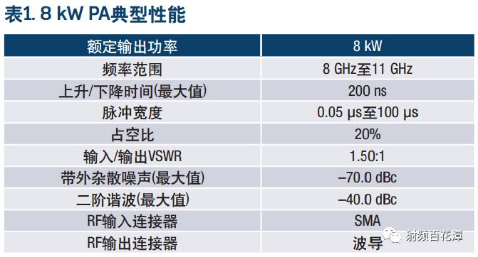
The 8kW amplifier topology is modular and includes four 2kW amplifier components whose output power is combined using a waveguide structure (Figure 1). The amplifier can be mounted in a standard 19-inch enclosure. The current design of the amplifier (Figure 2) is water cooled, and other air-cooled versions are under development. Table 1 gives a summary of the performance of water-cooled 8 kW GaN PA.
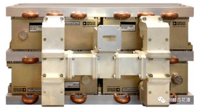
Figure 1. GaN-based solid-state power amplifier delivers 8 kW of output power and operates at X-band frequencies
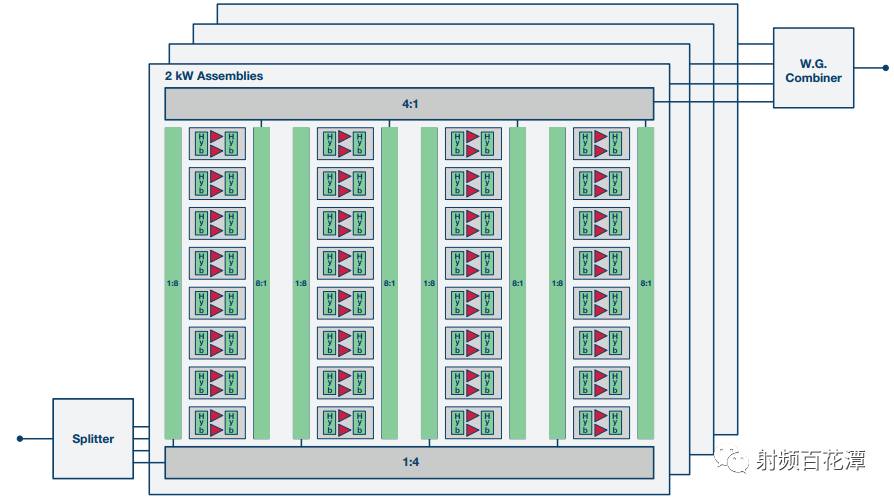
Figure 2. Block diagram of the structure and device of a GaN, X-band solid-state power amplifier
The 8 kW SSPA supports the consolidation of multiple modular SSPAs to produce higher power levels. An amplifier with three such 8 kW SSPA modules is currently being developed that achieves a peak output power level of 24 kW over the same frequency range. Other configurations that achieve a power level of 32 kW are also feasible and are currently being considered for further evaluation.
Analog Devices is currently developing an advanced power module that is also based on GaN technology and will have twice the RF/microwave output power of current modules. The module is sealed to support operation in extreme environments. Combined with the next-generation combined structure and lower insertion loss (compared to current methods), it will increase the pulse output power of the RF/microwave frequency to a level close to 75 kW to 100 kW. These advanced high-power SSPAs will include control and processor functions, support for fault monitoring, built-in test (BIT) functionality, remote diagnostic testing, and control of fast real-time bias control circuitry for MMIC devices that power amplifiers.
This type of GaN solid state power amplifier is designed to address the industry's need for wide instantaneous bandwidth, high output power amplifiers. Some systems attempt to meet these requirements with channelization or multiple amplifiers, each covering a portion of the desired spectrum and feeding into a multiplexer. This increases cost and complexity and results in gaps at the frequency crossover point of the multiplexer. A more efficient alternative solution is to continuously cover a wide frequency range at a higher power level, which has been achieved with two different GaN amplifiers covering VHF to L-band frequencies and 2 GHz to 18 GHz.
For VHF to S-band frequencies, Analog Devices has developed a very small, feature-rich, multi-octave amplifier that delivers 50 W of output power from 115 MHz to 2000 MHz. The amplifier achieves an output power level of 46 dBm (typically 40 W) when fed a nominal input signal of 0 dBm over the full frequency range.
The amplifier is available in a compact package measuring 7.3" x 3.6" x 1.4" with BIT capability for thermal and current overload protection and telemetry reporting, and integrated DC-DC converter for optimum RF performance with input supply range It is 26 VDC to 30 VDC. Figure 3 shows a photo of the amplifier. The relationship between the typical measured performance data of the output power and the frequency is shown in Figure 4.

Figure 3. Continuous wave (CW), 50 W, solid state power amplifier with an operating frequency range of 115 MHz to 2000 MHz
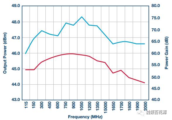
Figure 4. Output power vs. frequency for a 50 W, 115 MHz to 2000 MHz power amplifier

Figure 5. 50 W, CW output power amplifier with an operating frequency range of 2 GHz to 18 GHz
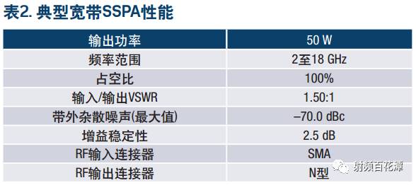
For broadband applications above 2 GHz, Analog Devices has also developed a GaN amplifier that produces 50 W continuous wave (CW) output power in the 2 GHz to 18 GHz band. This amplifier uses a commercial 10 W GaN MMIC, and its output power contribution is combined by a broadband low loss combined circuit. Multiple such amplifiers can also be combined to produce up to 200 W of output power over the same 2 GHz to 18 GHz bandwidth. The driver amplifier chain is also based on GaN active devices. The amplifier is powered by 48 VDC, has a built-in voltage regulator and high-speed switching circuitry to support pulse operation with good pulse fidelity and fast rise/fall times. Table 2 lists the specifications of this amplifier. Figure 5 shows a photograph of the amplifier, and Figure 6 shows the output power of the amplifier as a function of frequency (2 GHz to 18 GHz).
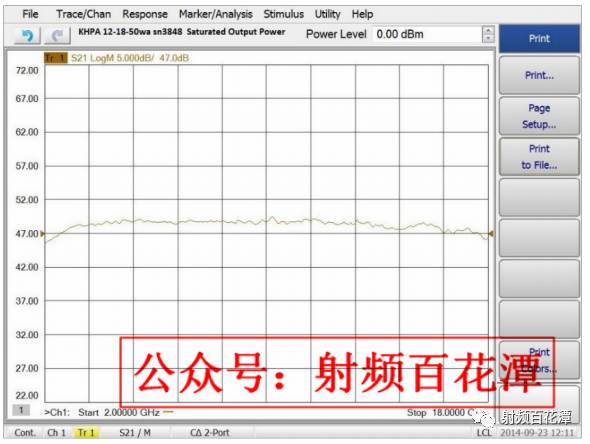
Figure 6. Output Power vs. Frequency for a 50 W, 2 GHz to 18 GHz Power Amplifier
This 50 W amplifier is part of a family of amplifiers from the 2 GHz to 18 GHz band. Analog Devices has also developed a compact benchtop amplifier with 12W output power (Figure 7) and a rack mount unit with 100W output power (Figure 8). Other amplifiers with frequencies ranging from 2 GHz to 6 GHz and from 6 GHz to 18 GHz are under development. Analog Devices is also working to increase the output power of these wideband amplifiers from current levels to 200 W and beyond. In order to achieve higher output power levels, Analog Devices is developing high-output power modules and wideband RF power combiners, which will greatly improve the combined efficiency and lower losses than current power combiners.
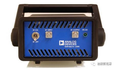
Figure 7. Broadband 2 GHz to 18 GHz power amplifier producing 12 W CW output power over the full frequency range

Figure 8. 2 GHz to 18 GHz solid state power amplifier producing 100 W CW output power over the full frequency range
The above are just a few examples of the level of performance that can be achieved with GaN solid state amplifiers. As more GaN semiconductor suppliers turn to larger sized wafers and the yield of each wafer continues to increase, the unit cost of such amplifiers is expected to decrease in the future. As the gate length is shortened, GaN-based SSPA will be able to support higher operating frequencies, so more and more GaN devices will be used in systems operating at millimeter wave frequencies. It is clear that the current trend of GaN to improve performance and reduce costs should last for some time.
We specialize in cable assembly overmolding. Our customized molded cables are built precisly following customers' spec.Experienced proposal can be offered to customers for evaluation by considering stable quality and competitive price.
Custom cable overmoldings improve the quality, look and functionality of many electrical cables. From battery interconnects and molded plugs to custom molded plugs and many other custom designed assemblies – ETOP is a premier custom cable overmolding supplier to OEMs.
we have internal design, prototype, and manufacturing the widest range of molded harnesses, also a diversified line of strain / flex reliefs and grommets.Molded Cables,Stranded Round Molded Cables,Molded Patch Cord Cable,4 Pole Waterproof Molded Cable,Waterproof Connectors
ETOP WIREHARNESS LIMITED , https://www.oemwireharness.com