
In high-speed signal circuit design, TI's signal conditioning products are widely used. The retimer class product involves register configuration, so its use is the most complicated. This article will take DS125DF1610 as an example to explain the circuit design and register configuration of retimer products.
The figure below is a typical application diagram in the DS125DF1610 product literature.
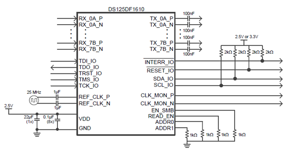
The hardware circuit design can be summarized into four key parts:
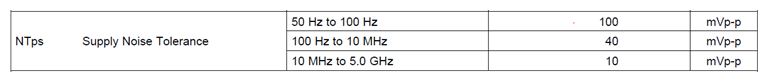
1. Power supply: TI's retimer products are very simple to supply, generally only need a 2.5V single power supply, like the DS125DF111 can also support a single 3.3V power supply. As can be seen from the table below, the retimer does not require high power supply noise performance. Generally, a DC/DC power supply scheme can be used, and an appropriate filter capacitor can be added to the power supply pin.
In addition, the power supply selection also needs to pay attention to the power consumption problem. In the chip data, the power consumption under various function combinations will be given, then we can calculate the maximum power consumption according to the actual application, as a reference for the power supply scheme selection. standard.
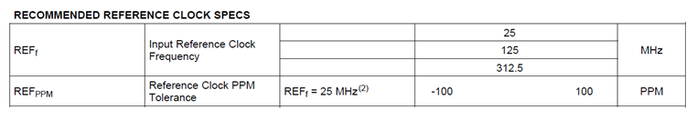
2. Clock: The external reference clock mainly provides a calibration reference for the retimer internal VCO. It only requires the frequency accuracy to be within +/-100ppm, and there is no special requirement for phase noise. It should be noted that the clock frequency and level supported by different retimers are different. Like the DS125DF1610 can support single-ended or differential inputs at 25 MHz, 125 MHz and 312.5 MHz, while most 10G retimers, such as the DS125DF111, only support 25MHz single-ended inputs. The design needs to be selected according to the data sheet.
3. AC coupling capacitor: High-speed signal transmission usually needs AC coupling. Considering the convenience of layout and signal integrity, TI part retimer products will integrate the coupling capacitor inside the chip. This needs to be confirmed from the product manual when designing. To avoid missing or repeated additions.
4. I / O port withstand voltage: As mentioned before, TI retimer is generally 2.5V single power supply, so you need to pay attention to its I / O port withstand voltage problem. In order to facilitate the docking with the on-board main control chip, the retimer internally handles the I2C, RESET and INTERRUPT ports, and allows the direct pull-up to 3.3V, which can be seen from the typical application diagram. Other I/O ports need to be careful not to exceed the power supply voltage.
Another important aspect of high-speed signal circuit design is the PCB layout, which directly affects the performance of signal transmission. When laying out, we need to pay attention to:
Reasonable distribution of signals, power and ground, the signal as far as possible from the noise source;
Maintain high-speed differential line symmetry and impedance control within 100Ω ± 5%;
Avoid sharp bending of differential lines, using 45° or curved bends;
Ensure skew match between different differential pairs.
Along the signal path, avoid the discontinuity of the reference plane and cause the impedance change, pay attention to the current return path;
The AC coupling capacitor can be selected from the 0402 package as much as possible. As much as possible, ensure that the trace width is consistent and minimize the number of vias.
The connector selected should meet the highest rate performance requirements.
When doing circuit design, as long as you notice the above mentioned places, you should be able to guarantee the normal power-on operation of the chip and the performance of the signal on the transmission link. What we need to do is register configuration. It should be noted that the optimal configuration order of the system after power-on is ASIC first, then retimer. This is because if the retimer is configured before the ASIC, then the data sent by the ASIC high-speed I/O port is unstable, and the retimer will try to lock as soon as it detects the signal. At this time, the adaptive parameters are not the most. Excellent.
The following is still taking the DS125DF1610 as an example. Assuming a 125MHz reference clock externally, the system needs to be compatible with 12.5Gbps and 6.25Gbps rates. The following table is the configuration flow we usually use.
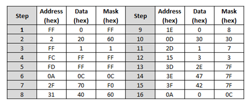
Before explaining the specific steps of the retimer configuration, you need to know what is the mask mode write. Because when configuring the register, only the bits that need to be configured can be modified, and other bits must be kept at the default value.
Taking step 2 as an example, a write operation with a mask of 0x60 is required for register 0x02, and the write value is 0x20. First, after the mask 0x60 is expanded, only bits 5 and 6 are 1, which means that we can only modify bits 5 and 6 of register 0x02, the value written is the bit value corresponding to data 0x20, and the other bits of the register are Leave the factory defaults unchanged.
The role of each step configuration will be described in detail below.
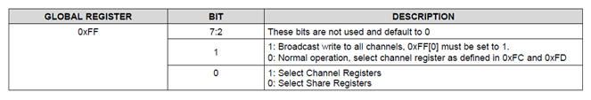
Step 1: Retimer internal registers are generally divided into two categories: shared registers and channel registers. Some global information like retimer, such as chip ID, external reference clock selection, etc. are in the shared register. So before configuring, be clear about which type of registers will be operated. Bit 0 of Register 0xFF is the selection.
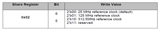
Step 2: The shared register is selected in step 1. Therefore, the operation of the 0x02 register is to select the external reference clock and select it according to the value given by the datasheet.
Step 3~5: The general shared register needs to operate to select the reference clock. All other configurations are in the channel register. First, Step 3 selects the channel register, and steps 4 and 5 select which channels will be modified at the same time. If all channels use the same configuration, the easiest way is to set bit 1 of 0xFF to 1, then all channels will be modified by broadcast, without having to configure the channel select register.
Step 6: Before configuring the channel register, put the CDR in the reset state to ensure that the retimer will not attempt to lock until the configuration is completed.
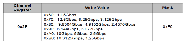
Step 7: There are two configurations for CDR lock rate. If the system rate is a common standard rate, such as the values ​​listed in the table below, then we can directly select the corresponding register value. But if it is not the standard rate, such as 11.3Gbps, then we need to manually calculate the VCO operating frequency. For the specific steps, please refer to section 8.3.2 of the DS125DF1610 product data.
Step 8: According to the difference between CTLE and DFE adaptive algorithms when CDR is locked, there are usually four working modes available. As shown in the following table, one of them can be selected by register 0x31 according to the debugging situation.
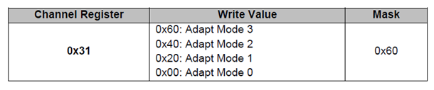
The specific differences between the four modes are as follows:
Mode 0: Manual mode, both CTLE and DFE need to be set manually;
Mode 1: CTLE is adaptive, and DFE needs to be set manually;
Mode 2: CTLE first adapts to an optimal setting, then DFE adaptively adjusts;
Mode 3: CTLE first adapts to a minimum required level, then DFE adapts to the optimal setting, and finally CTLE re-adapts to the optimal level.
Step 9: Determine whether DFE needs to be enabled according to the working mode selected in the previous step.
Step 10~15: The high-speed interface is adaptive only to the receiving side parameters, and the sending side parameters need to be manually set. Steps 10 through 15 are used to configure the retimer to send signal amplitude, emphasis, and FIR filters.
Step 16: Release the CDR reset.
Normally, after the above configuration is completed, the retimer can lock the work normally. If there is a bit error on the link during the test, you need to optimize each parameter according to the actual situation.
- Max efficiency 97.6% ,European efficiency 97.3%
- Max. Charge / Discharge Current 100A
-
Reasonable energy control to increase the proportion of
spontaneous use - With BMS system to ensure high battery life
- Natural cooling design
-
Compatible with lead-acid batteries and lithium battery energy
storage systems - Remote configuration and upgrade
On grid hybrid inverter working diagram:

Single Phase Hybrid Inverter,Dc To Ac Converter,Solar Power Inverter,On-Grid Solar Inverter
Hangzhou Saintish Technology Co.,Ltd. , https://www.saintishtech.com